Semiconductor device, method for operating a semiconductor device and method for manufacturing a semiconductor device

a semiconductor device and semiconductor technology, applied in the direction of semiconductor devices, basic electric elements, electrical equipment, etc., can solve the problems of dense trench devices being more susceptible to avalanche breakdown and useless devices

Active Publication Date: 2009-07-02
INFINEON TECH AG
View PDF8 Cites 38 Cited by
  • Summary
  • Abstract
  • Description
  • Claims
  • Application Information

AI Technical Summary

Problems solved by technology

Transient avalanche breakdowns frequently occur in demanding applications and can render a device useless.
While semiconductor devices of the trench dense concept exhibit improved properties regarding on-state resistance in comparison with standard devices of the field electrode concept, dense trench devices are more susceptible to avalanche breakdowns.

Method used


Image

  • Semiconductor device, method for operating a semiconductor device and method for manufacturing a semiconductor device
  • Semiconductor device, method for operating a semiconductor device and method for manufacturing a semiconductor device
  • Semiconductor device, method for operating a semiconductor device and method for manufacturing a semiconductor device

Examples


Embodiment Construction

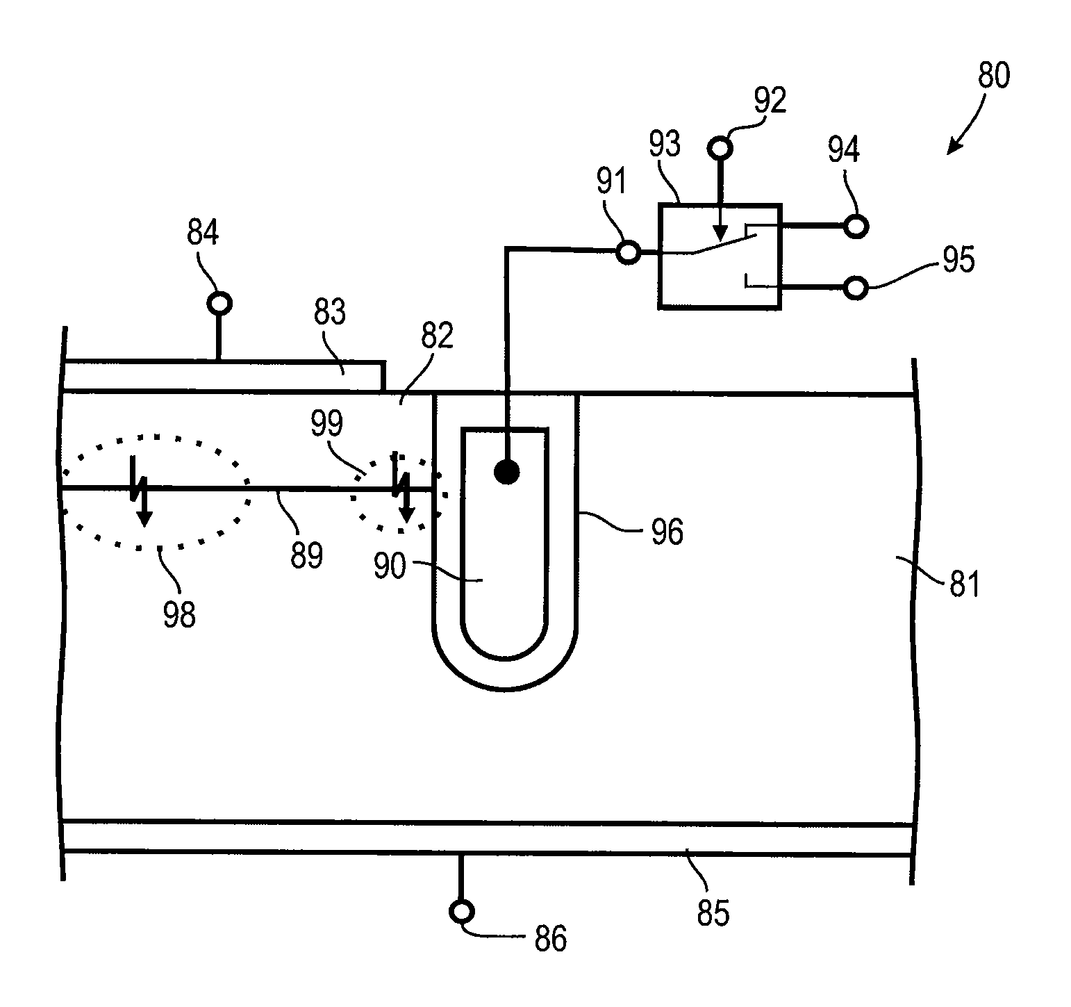
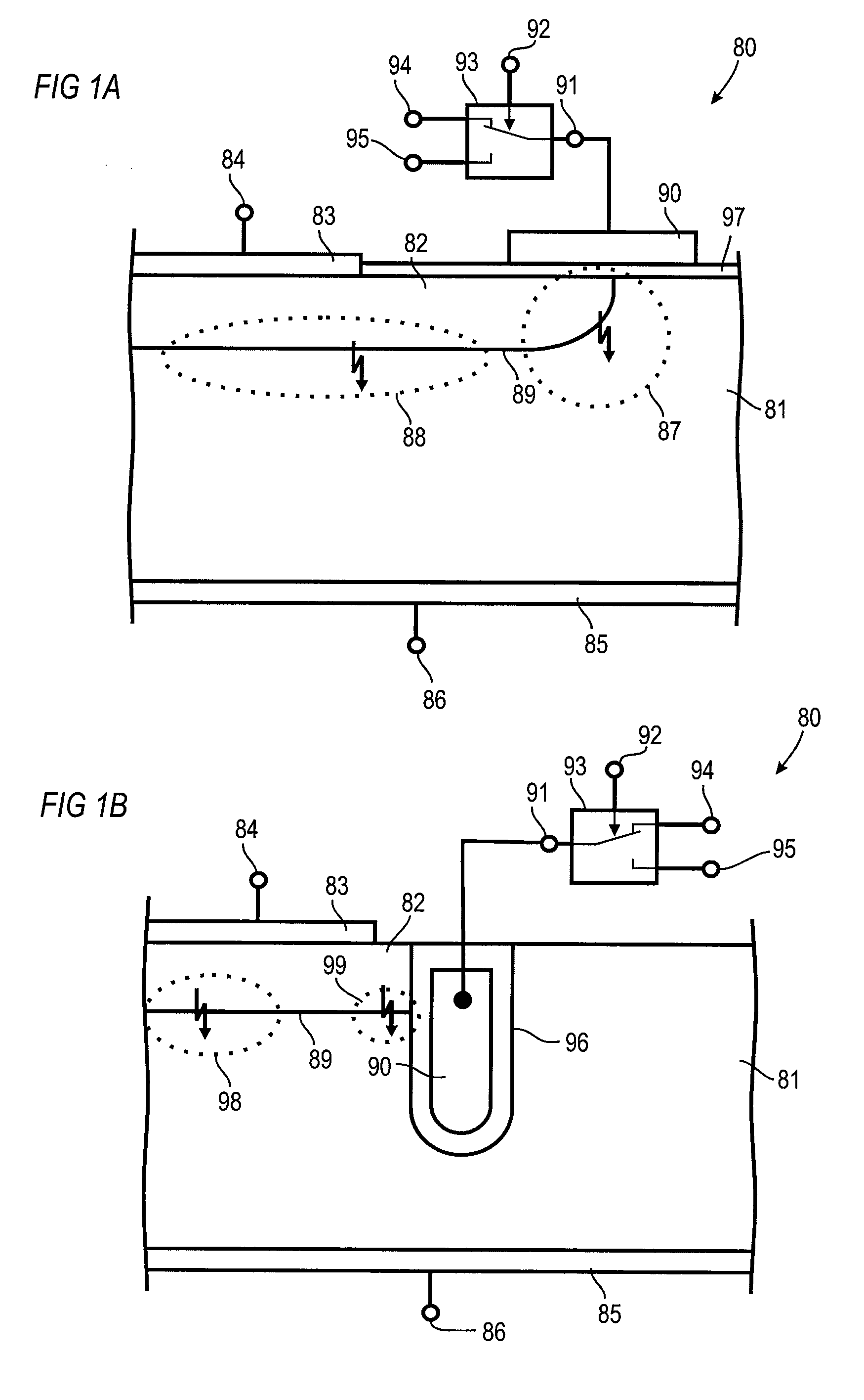
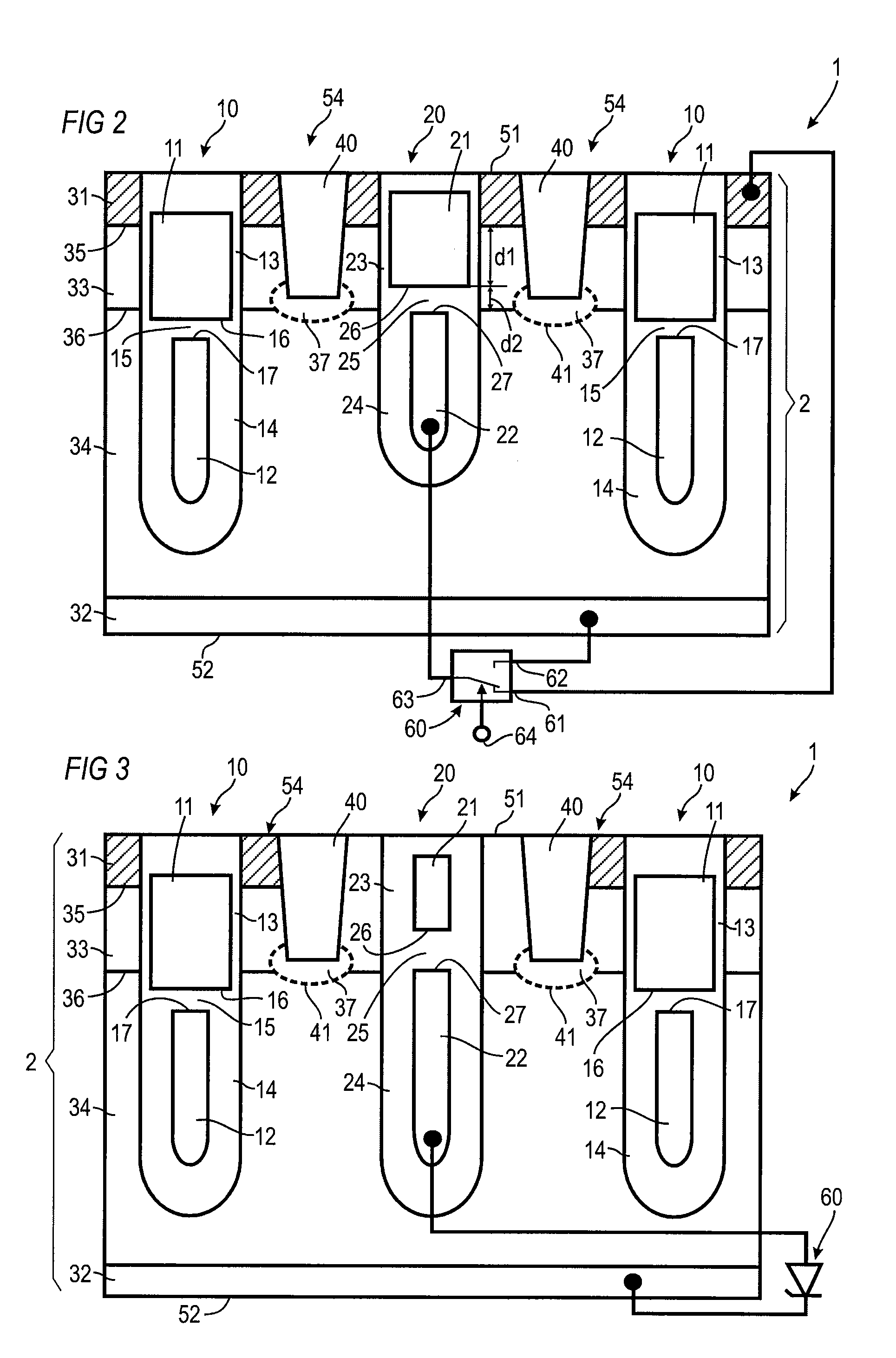
[0019]Reference will now be made in detail to various embodiments, one or more examples of which are illustrated in the figures. Each example is provided by way of explanation, and is not meant as a limitation of the invention. For example, features illustrated or described as part of one embodiment can be used on or in conjunction with other embodiments to yield yet a further embodiment. It is intended that the present invention includes such modifications and variations. The examples are described using specific language which should not be construed as limiting the scope of the appending claims. The drawings are not scaled and are for illustrative purposes only.

[0020]The term “lateral” as used in this specification intends to describe an orientation parallel to the main surface of a semiconductor wafer or die.

[0021]The term “vertical” as used in this specification intends to describe an orientation which is arranged perpendicular to the main surface of the semiconductor wafer or ...


PUM


Abstract

A semiconductor device includes a semiconductor substrate having at least a pn-junction arranged in the semiconductor substrate. At least a field electrode is arranged at least next to a portion of the pn-junction, wherein the field electrode is insulated from the semiconductor substrate. A switching device is electrically connected to the field electrode and adapted to apply selectively and dynamically one of a first electrical potential and a second electrical potential, which is different to the first electrical potential, to the field electrode to alter the avalanche breakdown characteristics of the pn-junction.

Description

FIELD OF THE INVENTION[0001]This description refers to embodiments of semiconductor devices and particularly power semiconductor devices with improved avalanche breakdown characteristics. Further embodiments refer to a method for operating a semiconductor device and a method for manufacturing a semiconductor device.BACKGROUND OF THE INVENTION[0002]Improvement of reliability and robustness of semiconductor devices is an ongoing aim in the development of semiconductor device and particularly power semiconductor devices. To ensure that devices which were delivered to customer meet the demands, the semiconductor devices are subjected to extended reliability tests before delivery. For example, the properties of the semiconductor device during an avalanche breakdown influence the reliability and are therefore subject for further developments. Transient avalanche breakdowns frequently occur in demanding applications and can render a device useless.[0003]Two main device concepts having diff...

Claims


Application Information

Patent Timeline
Patent Type & Authority Applications(United States)
IPC IPC(8): H01L29/78H01L21/336
CPCH01L29/402H01L29/407H01L29/41766H01L29/4236H01L29/42368H01L29/66727H01L29/66734H01L2924/0002H01L29/7397H01L29/7813H01L29/8611H01L29/8613H01L2924/00
Inventor ZUNDEL, MARKUS
Owner INFINEON TECH AG
Why Eureka
Try Eureka