Image sensor with vertical transfer gate

a technology of image sensor and transfer gate, which is applied in the field of image sensor, can solve the problems the and achieve the effect of increasing the overall size of the image sensor

Active Publication Date: 2011-04-28
STMICROELECTRONICS SRL
View PDF14 Cites 34 Cited by
  • Summary
  • Abstract
  • Description
  • Claims
  • Application Information

AI Technical Summary

Benefits of technology

[0009]It is one aim of embodiments of the present invention to a

Problems solved by technology

However, there are problems in increasing the size of N well 106 without limiting the ch

Method used


Image

  • Image sensor with vertical transfer gate
  • Image sensor with vertical transfer gate
  • Image sensor with vertical transfer gate

Examples


Embodiment Construction

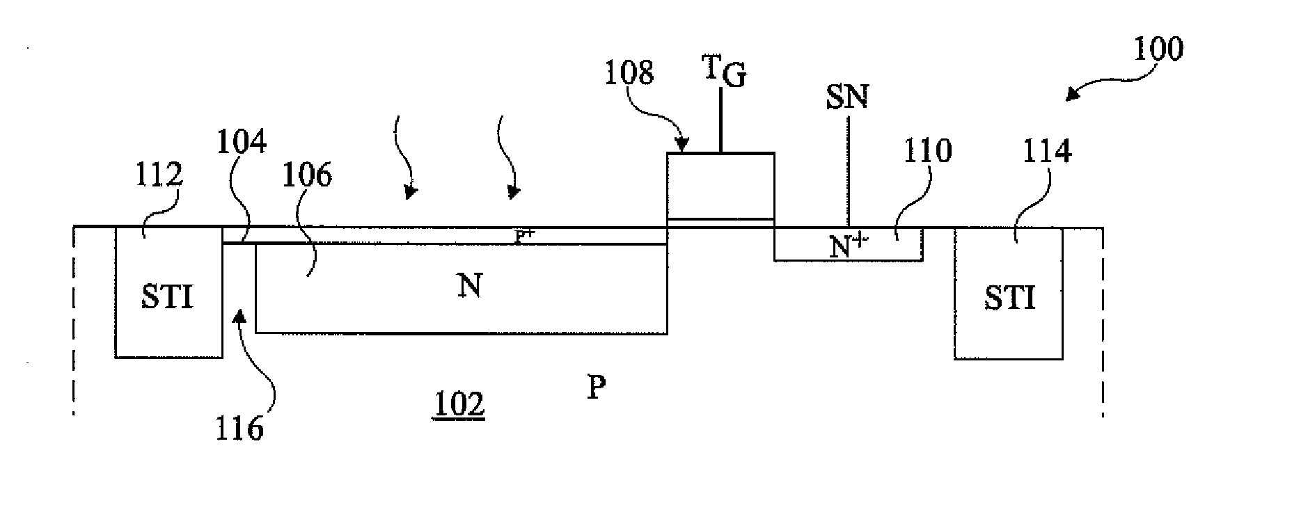
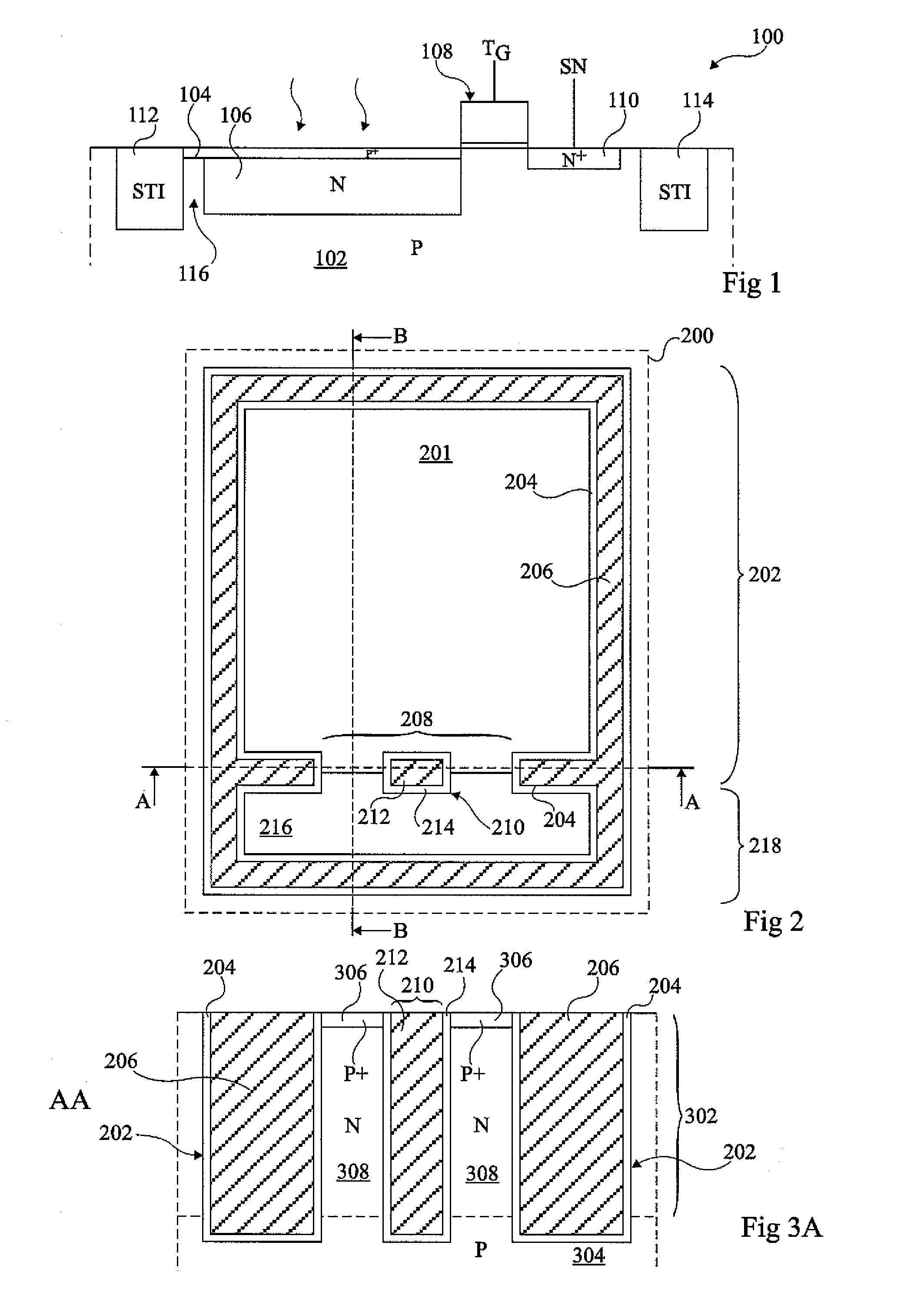
[0036]FIG. 2 is a plan view of a pixel 200 that has been proposed by the present applicant in French patent application FR 08 / 52759 and in U.S. patent application Ser. No. 12 / 429,413, which are hereby incorporated by reference to the maximum extent allowable by the law.

[0037]The pixel 200 comprises a rectangular photodiode region 201, which is, for example, around 1 μm square, surrounded by a rectangular trench 202. Trench 202 comprises an insulating layer 204, and a conducting core 206 formed of a conducting material.

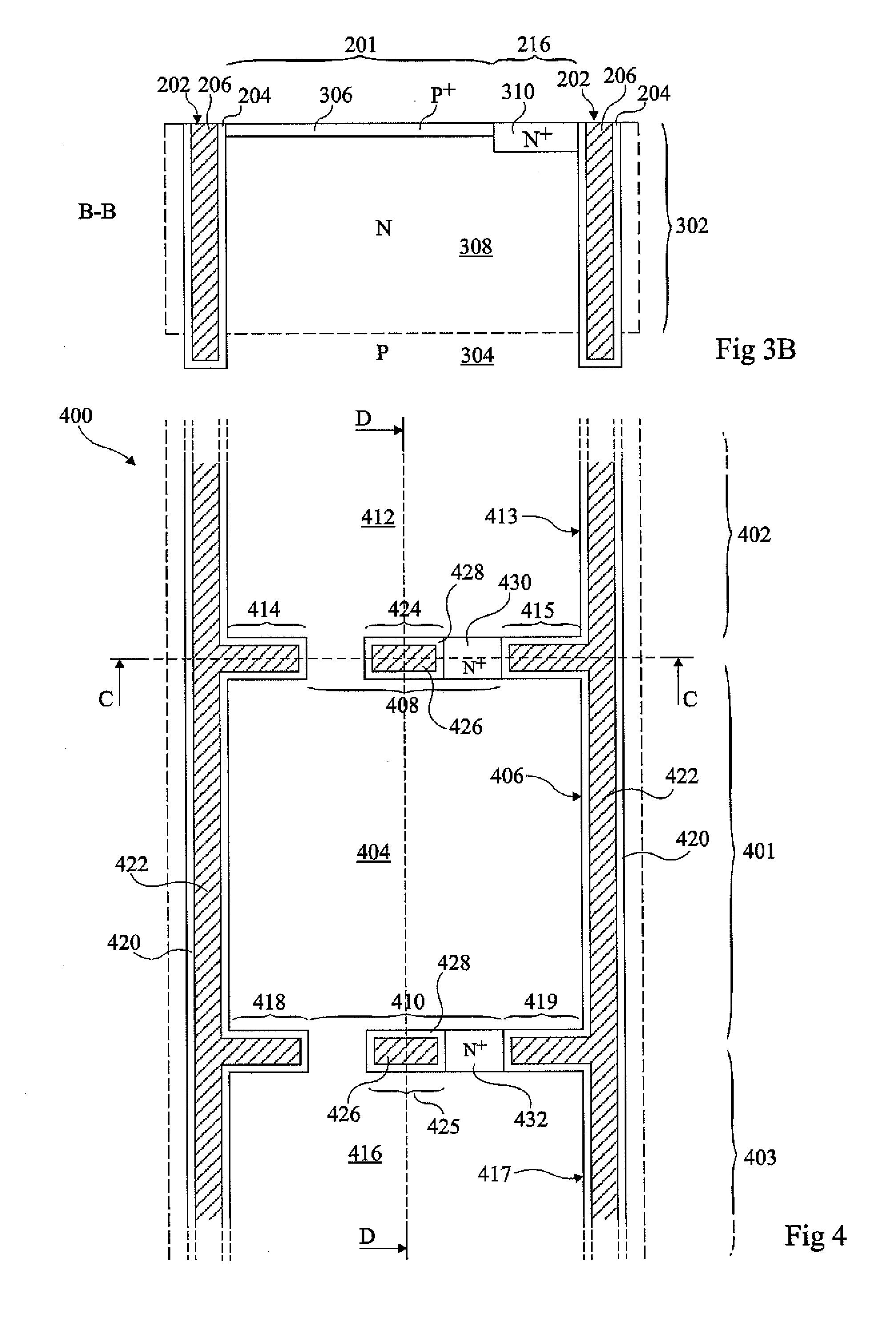
[0038]There is an opening 208 on one side of the rectangular trench. A charge transfer gate 210 is positioned approximately halfway across the opening 208, and comprises a rectangular column, for example having the same thickness as the trench 202. The column 210 comprises a conductive core 212 forming a gate electrode surrounded by an insulating layer 214 forming a gate insulation. The opening 208 leads to a charge collection region 216, which is surrounded by a recta...


PUM


Abstract

An image sensor including a first pixel positioned between second and third pixels, each of the first, second and third pixels comprising a photodiode region surrounded by an isolation trench; a first charge transfer gate comprising a first column electrode surrounded by an insulating layer and positioned in an opening of the isolation trench between the first and second pixels, the first column electrode being configured to receive a first transfer voltage signal; and a second charge transfer gate including a second column electrode surrounded by an insulating layer and positioned in an opening of the isolation trench between the first and third pixels, the second column electrode being configured to receive a second transfer voltage signal.

Description

CROSS REFERENCE TO RELATED APPLICATIONS[0001]This application claims the priority benefit of French patent application number 09 / 57427, filed on Oct. 22, 2009, entitled “Image Sensor With Vertical Transfer Gate,” which is hereby incorporated by reference to the maximum extent allowable by law.BACKGROUND OF THE INVENTION[0002]1. Field of the Invention[0003]The present invention relates to an image sensor, and in particular to an image sensor comprising pixels having a vertical transfer gate.[0004]2. Discussion of the Related Art[0005]Monolithic image sensors comprise photodiodes and transistors formed in a silicon substrate. More specifically, such image sensors comprise an array of pixels each having a photodiode coupled to a sense node via a transfer transistor. A charge accumulated by the photodiode during an integration period can be transferred to the sense node via the transfer transistor.[0006]FIG. 1 illustrates a pixel 100 of an image sensor formed in a P-type substrate 102. ...

Claims


Application Information

Patent Timeline
IPC IPC(8): H04N9/64
CPCH01L27/14603H01L27/1463H01L27/14641H01L27/14612H01L27/14683
Inventor ROY, FRANCOISBARBIER, FREDERIC
Owner STMICROELECTRONICS SRL
Why Eureka
Try Eureka