Semiconductor device, method for manufacturing same, and display device

a semiconductor layer and display device technology, applied in non-linear optics, instruments, optics, etc., can solve the problem that conventional components cannot be combined, and achieve the effect of suppressing increasing surface recesses and projections of semiconductor layers, and improving light usage efficiency of optical sensors

Inactive Publication Date: 2011-11-10
SHARP KK
View PDF3 Cites 23 Cited by
  • Summary
  • Abstract
  • Description
  • Claims
  • Application Information

AI Technical Summary

Benefits of technology

[0023]According to the present invention, in a semiconductor device equipped with a TFT and a TFD that are formed on the same substrate, semiconductor layers for the TFT and the TFD can be optimized in accordance with the device characteristics respectively required for them. Therefore, it becomes possible to achieve each of the device characteristics required for the TFT and the TFD.
[0024]Moreover, because it is possible to increase surface recesses and projections of the semiconductor layer for the TFD, when using the TFD as an optical sensor, light usa

Problems solved by technology

Further, it also becomes possible to achieve a product including new fu

Method used


Image

  • Semiconductor device, method for manufacturing same, and display device
  • Semiconductor device, method for manufacturing same, and display device
  • Semiconductor device, method for manufacturing same, and display device

Examples


embodiment 1

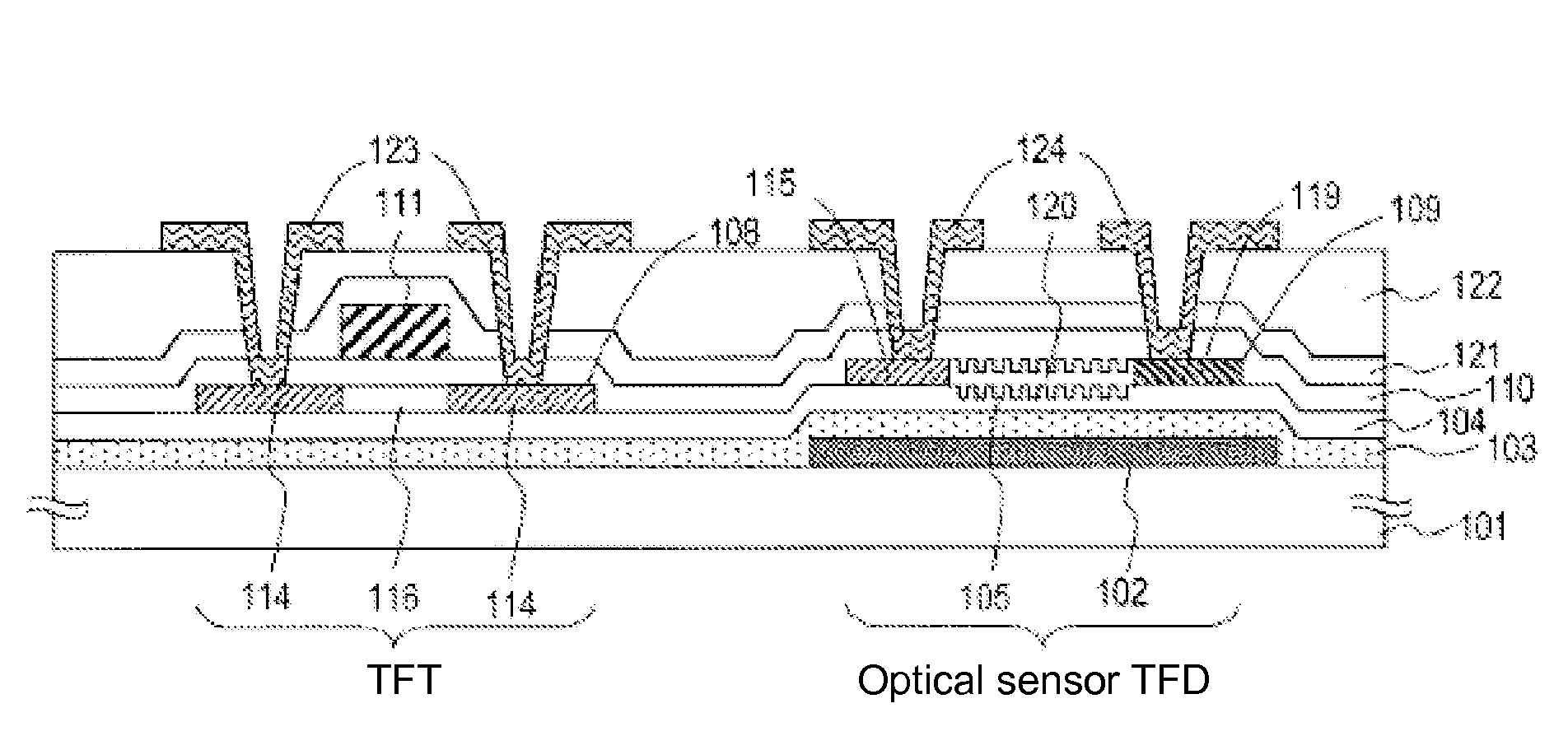
[0045]Embodiment 1 of a semiconductor device according to the present invention will be described below with reference to figures. The semiconductor device of the present embodiment includes n-channel type TFTs and optical sensor TFDs formed on the same substrate, and is used as an active matrix display device, for example.

[0046]FIG. 1 is a schematic cross-sectional view showing an example of a semiconductor device according to the present embodiment. The semiconductor device of the present embodiment typically includes a plurality of TFTs and a plurality of TFDs formed on the same substrate, but for simplification, the structure of only a single TFT and a single TFD is shown here. Further, an n-channel type TFT having a single drain structure is shown as an example of the TFT, but the structure of the TFT is not limited to this. A TFT having an LDD structure or a GOLD structure may also be formed, or a plurality of TFTs including n-channel type TFTs and p-channel type TFTs may be f...

embodiment 2

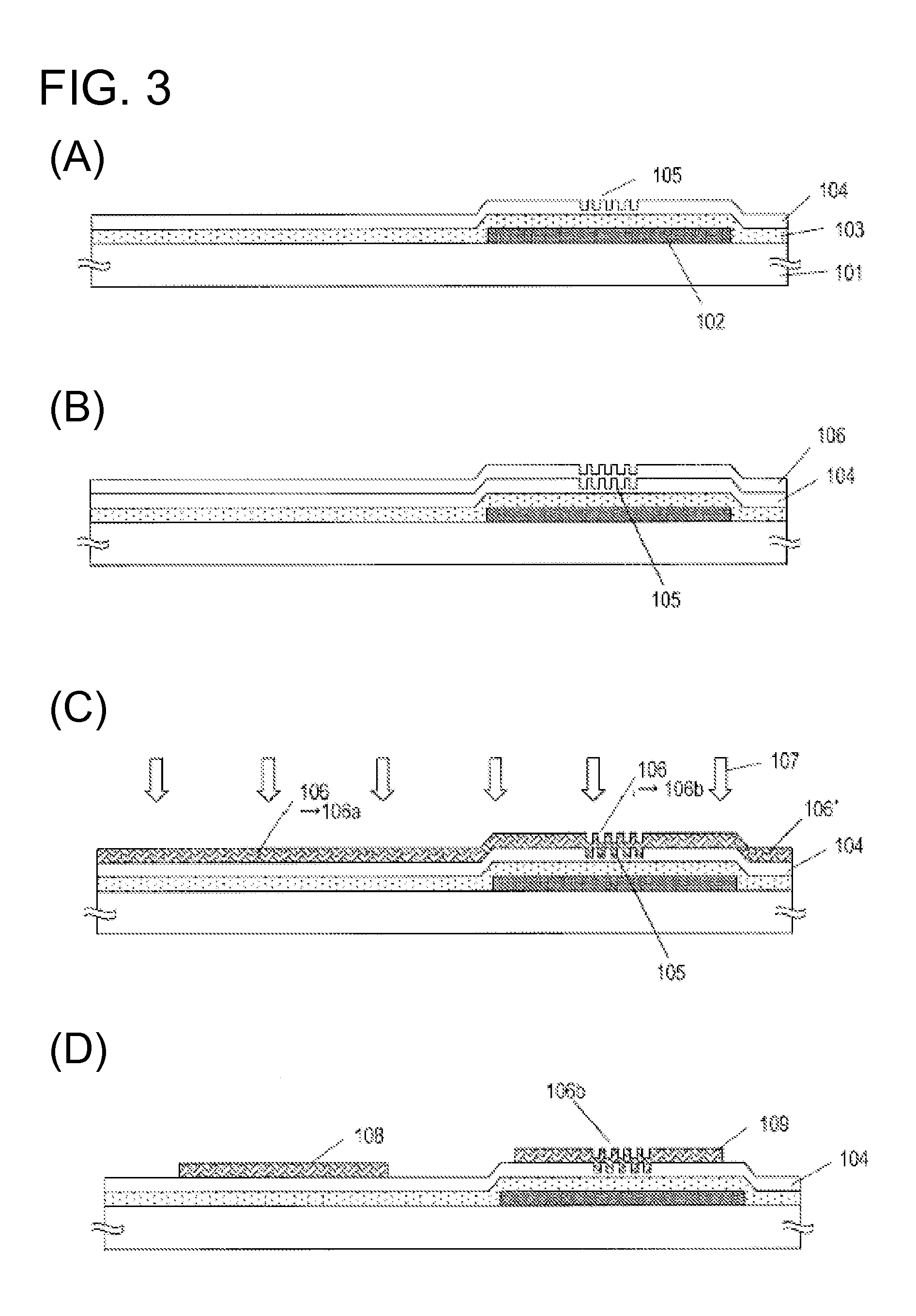
[0077]Next, Embodiment 2 of the semiconductor device according to the present invention will be described. The semiconductor device of the present embodiment includes a structure similar to the semiconductor device of Embodiment 1 (FIG. 1). However, an amorphous semiconductor film is crystallized using catalytic element in the present embodiment, which is an aspect different from the method for manufacturing the semiconductor device in Embodiment 1.

[0078]An example of the method for manufacturing the semiconductor device of the present embodiment will be described below with reference to figures.

[0079]First, as shown in FIG. 5(A), a light-shielding layer 202 is formed and patterned on a substrate 201, and insulating layers 203 and 204, which will be the base films, are formed. A silicon nitride film 203 and a silicon oxide film 204 are formed here. A recessed and projected pattern 205 is then formed in the silicon oxide film 204. The forming method is similar to the method described...

embodiment 3

[0093]Display devices having a sensor function will be described in the present embodiment. These display devices are configured using a semiconductor device according to any one of the above-described embodiments.

[0094]A display device having a sensor function of the present embodiment is a liquid crystal display device with a touch sensor, for example, and includes a display region and a frame region located around the display region. The display region includes a plurality of display parts (pixels) and a plurality of optical sensor parts. The respective display parts include a pixel electrode and a pixel switching TFT, and the respective optical sensor parts include a TFD. The frame region has a display-use driver circuit for driving the respective display parts, and driver circuit-use TFTs are used in the driver circuit. The pixel switching TFT, the driver circuit-use TFT, and the TFD of the optical sensor part are formed on the same substrate by a method such as the methods des...


PUM


Abstract

Disclosed is a semiconductor device in which a thin film transistor and a thin film diode are provided on one same substrate, and the characteristics respectively required for the thin film transistor and the thin film diode are achieved. Specifically disclosed is a semiconductor device that includes an insulating layer (104) formed on the surface of a substrate (101), and a thin film transistor and a thin film diode that are formed on the insulating layer (104). A portion of the surface of the insulating layer (104), which is positioned below a semiconductor layer (109) for the thin film diode, is provided with a first recessed and projected pattern (105). Meanwhile, a portion of the surface of the insulating layer (104), which is positioned below a semiconductor layer (108) for the thin film transistor, is not provided with the first recessed and projected pattern (105). The surface of the semiconductor layer (109) for the thin film diode has a second recessed and projected pattern that reflects the shape of the first recessed and projected pattern (105).

Description

TECHNICAL FIELD[0001]The present invention relates to a semiconductor device including a thin film transistor (TFT) and a thin film diode (TFD), a method for manufacturing the same, and a display device including a thin film transistor and a thin film diode.BACKGROUND ART[0002]In recent years, development of semiconductor devices in which a thin film transistor (TFT) and a thin film diode (TFD) are formed on the same substrate, and electronic devices including such a semiconductor device have been promoted. As for the method of manufacturing such a semiconductor device, there has been suggested a method of forming a semiconductor layer for a TFT and a TFD using the same crystalline semiconductor film formed over the substrate.[0003]Patent Document 1 discloses an image sensor, which includes an optical sensor part using a TFD and a driver circuit using a TFT on a same substrate. In Patent Document 1, an amorphous semiconductor film formed on the substrate is crystallized to form the ...

Claims


Application Information

Patent Timeline
IPC IPC(8): G06F3/041H01L21/20H05B37/02H01L29/786
CPCG02F1/1365G02F1/1368G06F3/0412H01L27/14632H01L27/1214H01L27/14621G06F3/042
Inventor NAKATSUJI, HIROSHI
Owner SHARP KK
Why Eureka
Try Eureka