Charge-trapping layer with optimized number of charge-trapping sites for fast program and erase of a memory cell in a 3-dimensional nor memory string array

a memory cell and charge-trapping layer technology, applied in the direction of semiconductor devices, electrical devices, transistors, etc., can solve the problems of reducing the endurance of the charge-trapping layer, increasing the overall program and erase time, and reducing the endurance of the memory device. , the effect of reducing the programming and erase tim

Active Publication Date: 2021-10-14
SUNRISE MEMORY CORP
View PDF1 Cites 0 Cited by
  • Summary
  • Abstract
  • Description
  • Claims
  • Application Information

AI Technical Summary

Benefits of technology

[0010]The present invention provides an optimized charge-trapping layer in a memory device which allows a memory system incorporating such memory devices to have reduced programming and erase times. The optimized charge-trapping layer may be applicable, for example, to memory cells in a 3-dimensional array of non-volatile NOR-type memory strings. The parameters to be optimized include, for example, the number of charge-trapping sites in the charge-trapping layer, and its physical dimensions (e.g., length, width, and thickness). Furthermore, the electric field across the tunnel oxide layer during the programming or erase operational for the optimized charge-trapping layer is significantly lower than under a conventional programming or erase operation, such that the endurance of the memory device is significantly enhanced.

Problems solved by technology

However, a higher voltage at the gate conductor decreases the charge-trapping layer's endurance.
In either case, using a minimal program or erase pulse may not succeed in programming or erasing any given memory cell to threshold voltage Vp or Ve, respectively.
While the read-verify procedure is effective in achieving distributions of reduced widths using lower (in magnitude) program or erase voltage, overall program and erase times are increased because of the inevitable repetitive program and erase steps.

Method used


Image

  • Charge-trapping layer with optimized number of charge-trapping sites for fast program and erase of a memory cell in a 3-dimensional nor memory string array
  • Charge-trapping layer with optimized number of charge-trapping sites for fast program and erase of a memory cell in a 3-dimensional nor memory string array
  • Charge-trapping layer with optimized number of charge-trapping sites for fast program and erase of a memory cell in a 3-dimensional nor memory string array

Examples


Embodiment Construction

lass="d_n">[0019]In this detailed description, process steps described in one embodiment may be used in a different embodiment, even if those steps are not described in the different embodiment. When reference is made herein to a method having two or more defined steps, the defined steps can be carried out in any order or simultaneously (except where context or specific instruction excludes that possibility), and the method can include one or more other steps carried out before any of the defined steps, between two of the defined steps, or after all the defined steps (except where context excludes that possibility).

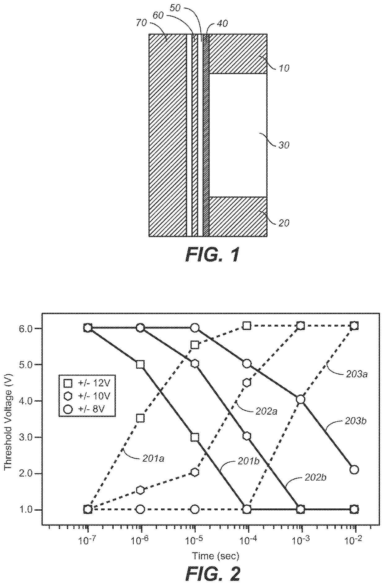
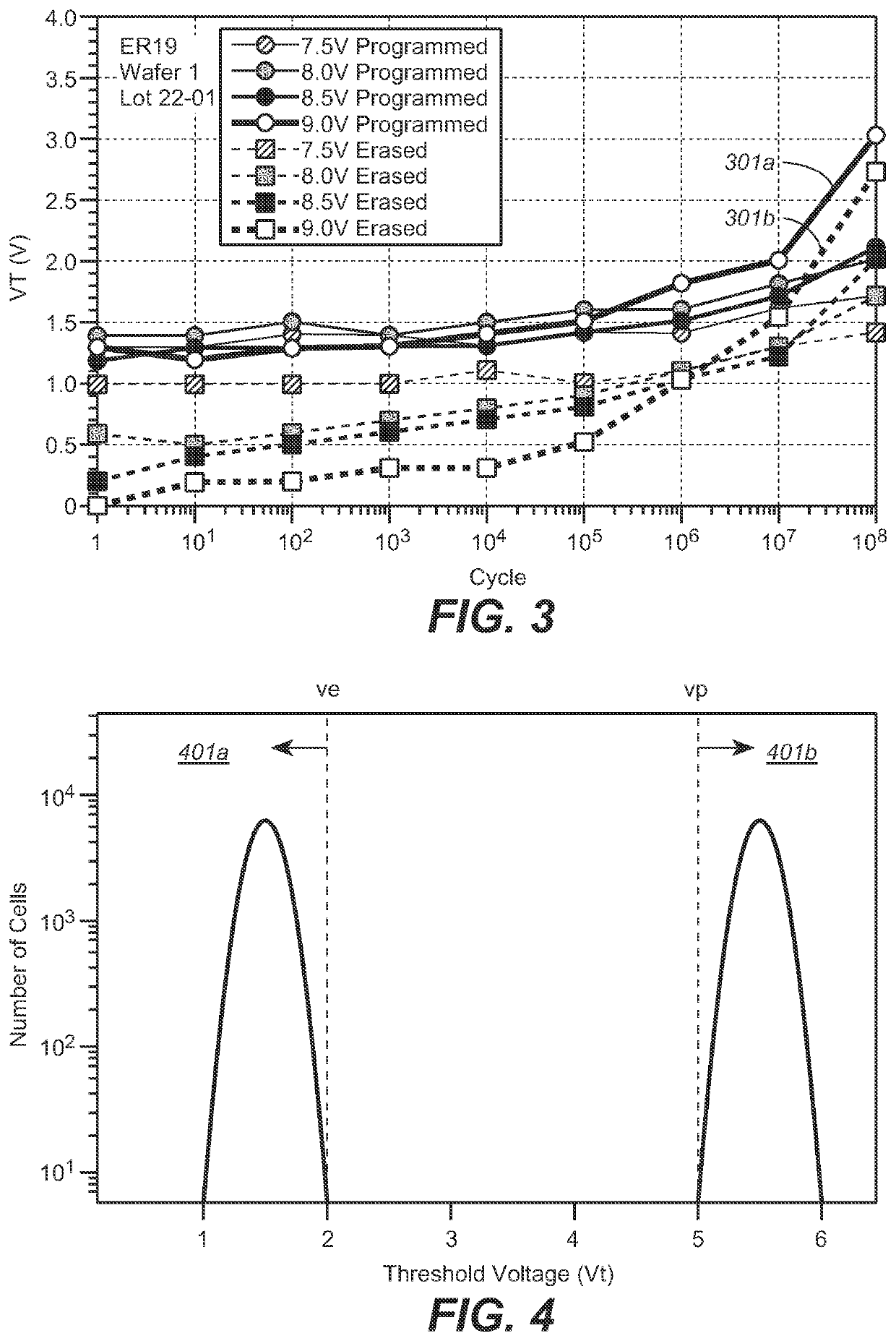
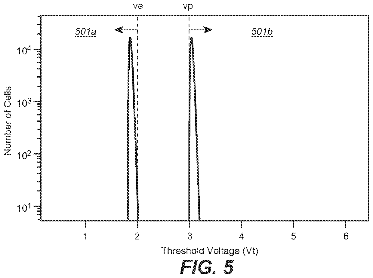
[0020]According to one embodiment of the present invention, the distribution of threshold voltages of memory cells in a “programmed” or an “erased” state may be reduced by limiting the available number of charge-trapping sites needed to obtain a threshold voltage difference of ΔVt between memory cells of the “programmed” and “erased” states. FIG. 5 shows narrow distributi...


PUM

PropertyMeasurementUnit
refractive indexaaaaaaaaaa
voltageaaaaaaaaaa
voltageaaaaaaaaaa

Abstract

A thin-film memory transistor includes a source region, a drain region, a channel region, a gate electrode, and a charge-trapping layer provided between the channel region and the gate electrode and electrically isolated therefrom, wherein the charge-trapping layer has includes a number of charge-trapping sites that is 70% occupied or evacuated using a single voltage pulse of a predetermined width of 500 nanoseconds or less and a magnitude of 15.0 volts or less. The charge-trapping layer comprises silicon-rich nitride may have a refractive index of 2.05 or greater or comprises nano-crystals of germanium (Ge), zirconium oxide (ZrO2), or zinc oxide (ZnO). The thin-film memory transistor may be implemented, for example, in a 3-dimensional array of NOR memory strings formed above a planar surface of a semiconductor substrate.

Description

CROSS REFERENCE TO RELATED APPLICATIONS[0001]This application is related to and claims priority of U.S. provisional application application no. 63 / 007,244, filed on Apr. 8, 2020. The priority of this application is expressly claimed, and the disclosure is hereby incorporated by reference in their entirety[0002]The present application is related to U.S. patent application (“Related Application”), Ser. No. 16 / 744,067, entitled “Implementing Logic Function And Generating Analog Signals Using NOR Memory Strings,” filed on Jan. 15, 2020, which is a continuation-in-part application of U.S. non-provisional patent application Ser. No. 16 / 582,996 (“Non-provisional Application I”), entitled “Memory Circuit, System and Method for Rapid Retrieval of Data Sets,” filed on Sep. 25, 2019, which is a continuation application of U.S. non-provisional patent application (“Non-Provisional Application II”), Ser. No. 16 / 107,306, entitled “System Controller and Method for Determining the Location of the Mo...

Claims


Application Information

Patent Timeline
Patent Type & Authority Applications(United States)
IPC IPC(8): H01L29/423H01L27/11568H01L29/786H01L29/792
CPCH01L29/42348H01L27/11568H01L29/7926H01L29/78672H01L29/78642H10B43/30
Inventor CHIEN, WU-YI HENRYHERNER, SCOTT BRADHARARI, ELI
Owner SUNRISE MEMORY CORP
Why Eureka
Try Eureka