Method and apparatus for potting an electronic device

a technology for electronic devices and potting equipment, which is applied in the direction of electrical apparatus construction details, electrical apparatus casings/cabinets/drawers, instruments, etc., can solve the problems of waste of packaging materials beyond the required amount to seal the device from the environment, inefficient potting process, and unnecessarily high cos

Active Publication Date: 2013-05-30
ENPHASE ENERGY
View PDF5 Cites 3 Cited by
  • Summary
  • Abstract
  • Description
  • Claims
  • Application Information

AI Technical Summary

Benefits of technology

The present invention provides a method and apparatus for potting an electronic device. The method involves placing a fill control element in an enclosure with the electronic device, and then filling the remaining space in the enclosure with a sealant to trap air. The technical effect of this invention is to provide a more efficient and effective way to protect electronic devices from damage and contamination during transportation and usage.

Problems solved by technology

For example, electronic devices utilized in systems for generating energy from renewable resources, such as solar power systems, wind farms, hydroelectric systems, or the like, may be exposed to environment elements and therefore require packaging.
Unfortunately, an excess amount of packaging material beyond that required to seal the device from the environment is wasted during the potting process.
Thus, the potting process is inefficient and unnecessarily expensive.

Method used


Image

  • Method and apparatus for potting an electronic device
  • Method and apparatus for potting an electronic device
  • Method and apparatus for potting an electronic device

Examples


Embodiment Construction

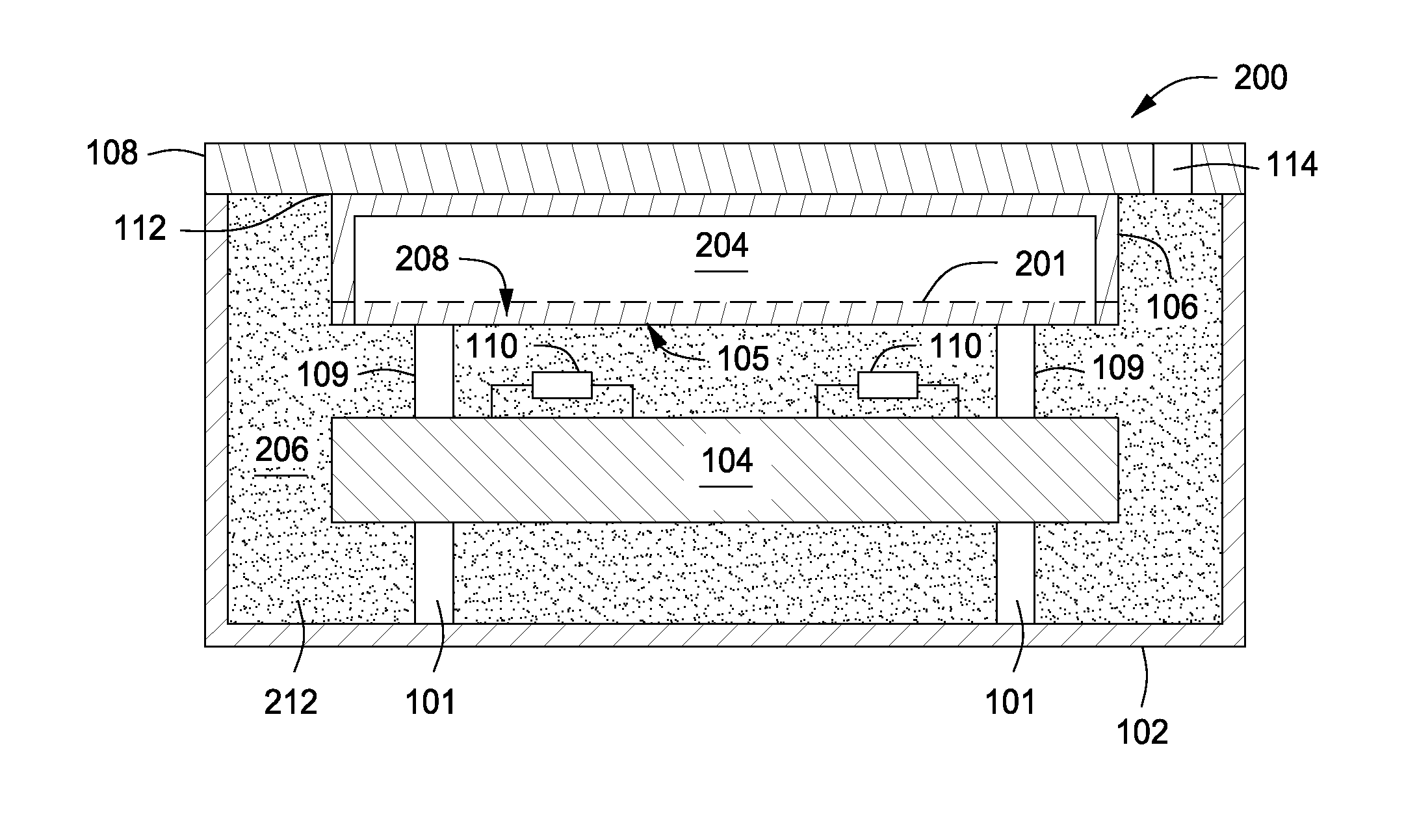
[0015]A method and apparatus for potting an electronic device are provided herein. One embodiment of an inventive method may advantageously provide an efficient, cost effective technique for potting an electronic device, such as a printed circuit (PC) board or other suitable device by reducing the amount of sealant used in potting the device. One exemplary means of improved potting comprises a device enclosure and a fill control element.

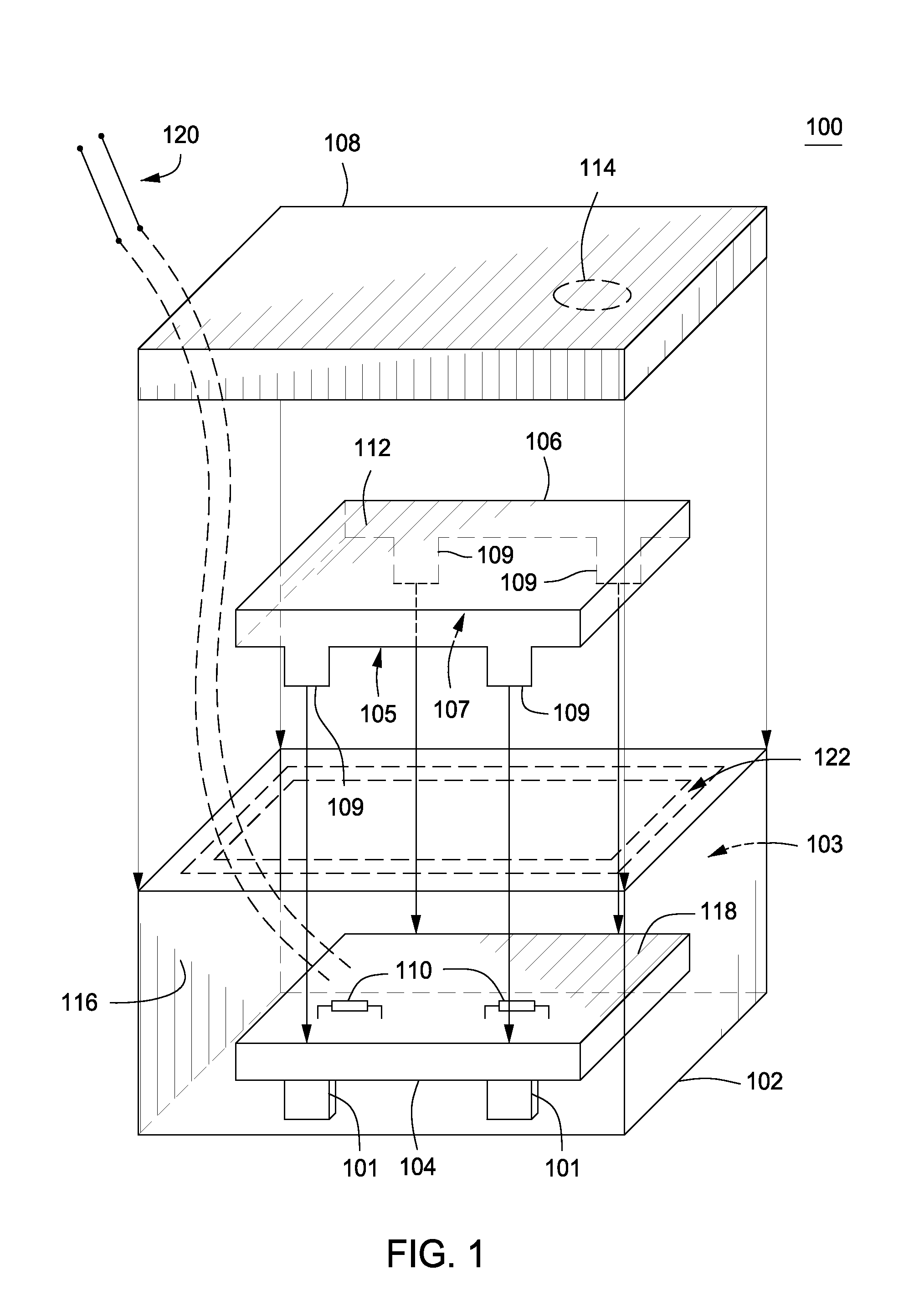
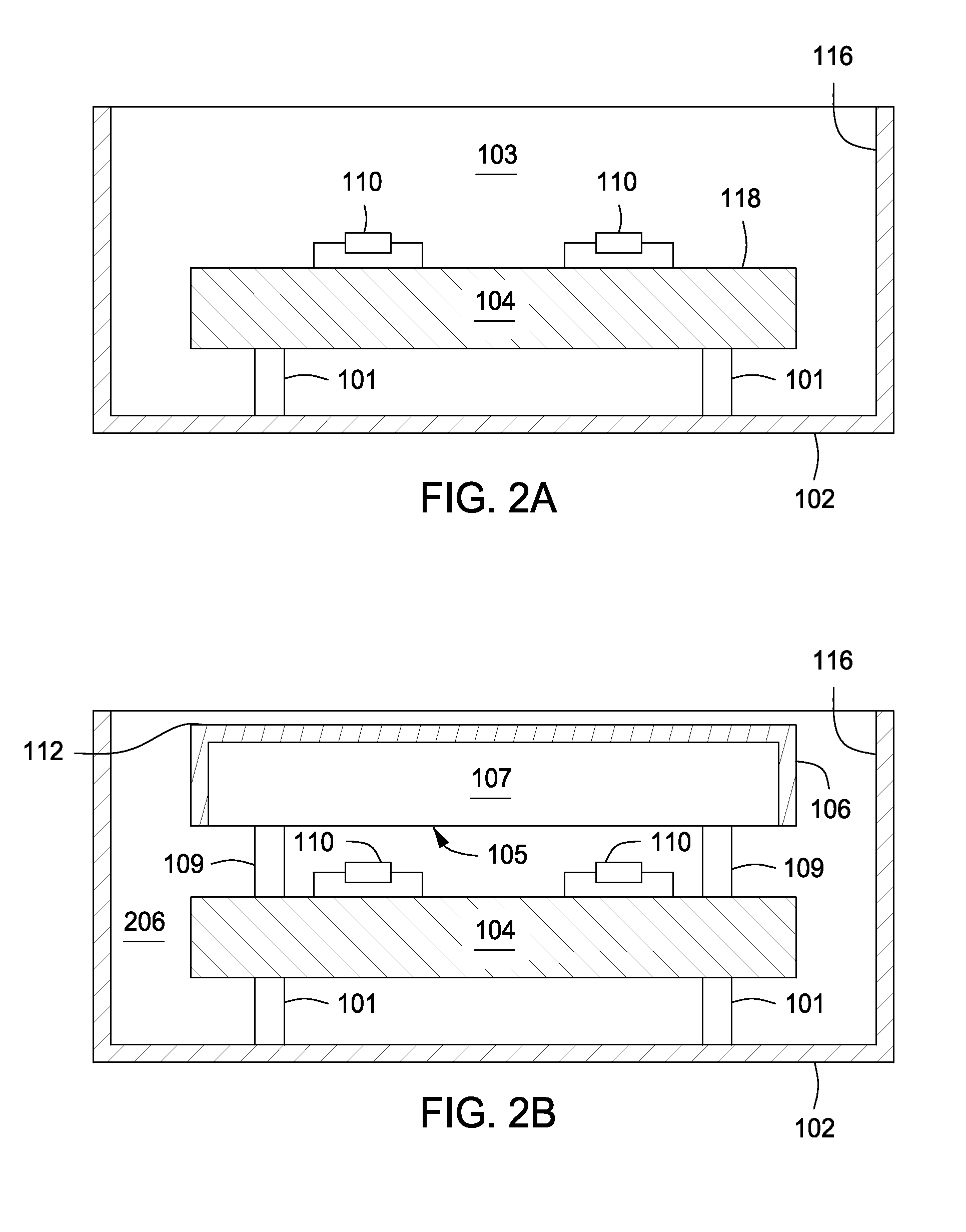
[0016]FIG. 1 depicts a perspective, exploded view of an assembly 100 for potting an electronic device in accordance with some embodiments of the present invention. The assembly 100 includes an enclosure 102 having a first inner volume 103 with an electronic device 104 disposed therein. A fill control element 106 may be disposed atop the electronic device 104, where the fill control element 106 has a second inner volume 107 and an opening 105 that faces the electronic device 104. The opening 105 allows the first inner volume 103 to be fluidly coupled ...


PUM


Abstract

Method and apparatus for potting an electronic device. In one embodiment, the method comprises providing an enclosure having a first inner volume with the electronic device disposed therein; placing a fill control element within the enclosure such that a second inner volume of the fill control element is fluidly coupled to the first inner volume; and filling a remaining portion of the first inner volume, the remaining portion not occupied by the electronic device or the fill control element, with a sealant such that air is trapped within at least a first portion of the second inner volume.

Description

CROSS-REFERENCE TO RELATED APPLICATIONS[0001]The present invention is a continuation of co-pending U.S. patent application Ser. No. 12 / 657,071, filed Jan. 13, 2010, which claims the benefit of the U.S. provisional patent application Ser. No. 61 / 204,929, filed Jan. 13, 2009. Each of the aforementioned patent applications is herein incorporated in its entirety by reference.BACKGROUND OF THE INVENTION[0002]1. Field of the Invention[0003]Embodiments of the present invention generally relate to an electronic device, and more particularly, relate to a method and apparatus for potting an electronic device, for example, a printed circuit (PC) board.[0004]2. Description of the Related Art[0005]Some devices, such as electronics devices, may require packaging to prevent exposure to an environment comprising one or more of air, moisture, salt, acid, or the like. For example, electronic devices utilized in systems for generating energy from renewable resources, such as solar power systems, wind ...

Claims


Application Information

Patent Timeline
Patent Type & Authority Applications(United States)
IPC IPC(8): H05K5/06
CPCH05K3/284H05K2203/1316H05K5/064
Inventor FORNAGE, MARTIN
Owner ENPHASE ENERGY
Why Eureka
Try Eureka