Unlock instant, AI-driven research and patent intelligence for your innovation.
Light-Emitting Device
Active Publication Date: 2014-10-16
SEMICON ENERGY LAB CO LTD
View PDF37 Cites 45 Cited by
Summary
Abstract
Description
Claims
Application Information
AI Technical Summary
This helps you quickly interpret patents by identifying the three key elements:
Problems solved by technology
Method used
Benefits of technology
The invention provides a light-emitting device with a reflective electrode that has increased irregularity on its surface shape. This prevents interference fringes and reflection of images caused by external light. Additionally, the device allows for a larger screen and higher definition, as the surface shape of the reflective electrode is improved.
Problems solved by technology
Thus, there is a problem in that these reflective electrodes function like mirrors and reflect an image in the screen.
Further, the regular arrangement of the reflective electrodes might cause diffraction of light reflected by each reflective electrode, so that interference fringes might appear on the screen.
Method used
Image
Click on the blue label to locate the original text in one second.
Reading with bidirectional positioning of images and text.
Examples
embodiment 1
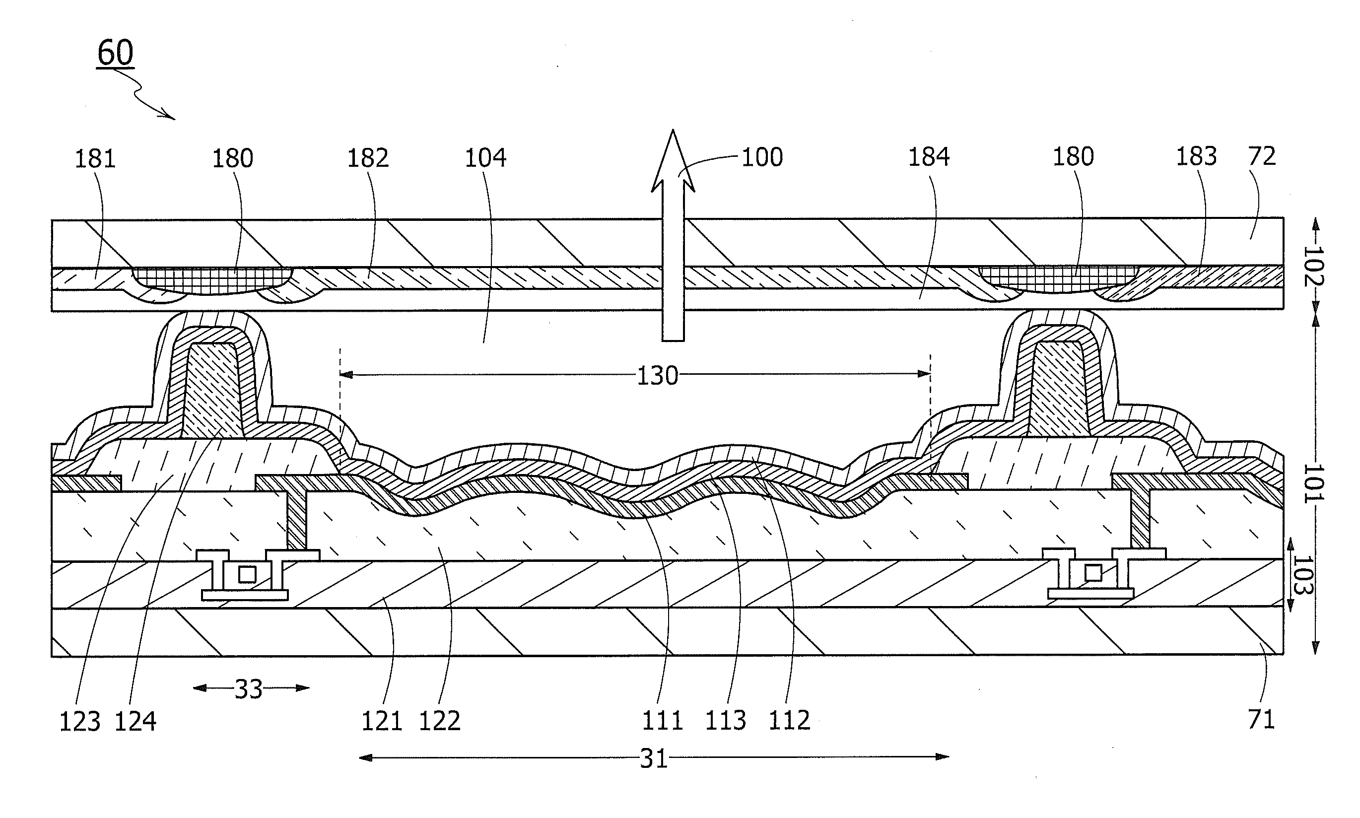
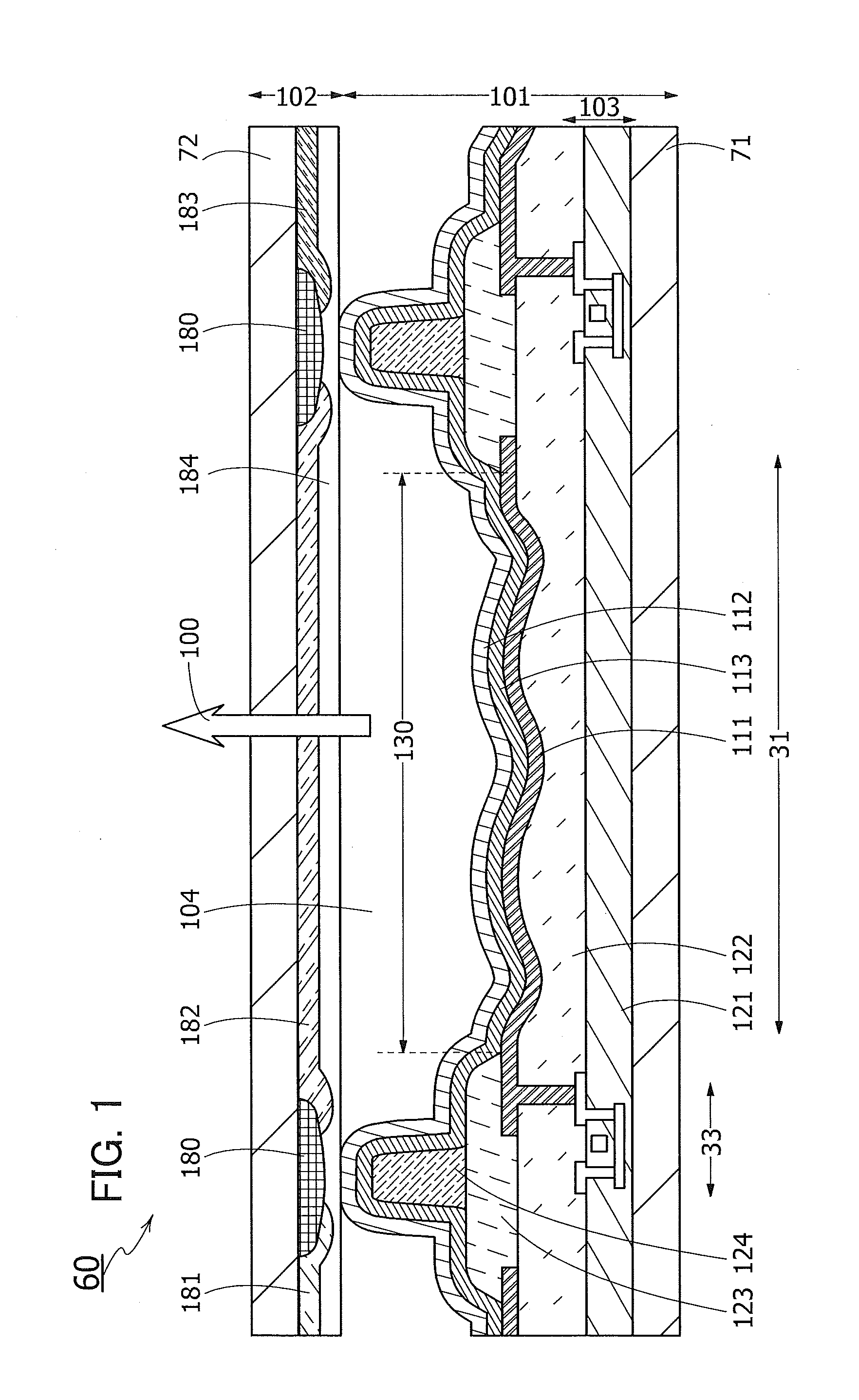
[0027]This embodiment will be described with reference to FIG. 1, FIGS. 2A to 2C, and FIGS. 3A to 3C. In this embodiment, an active matrixelectroluminescencedisplay device will be described as an example of a light-emitting device. An EL display device is a light-emitting device including an EL panel, a controller, a power supply circuit, and the like and is also a semiconductor device.
[0028]FIG. 3A is a block diagram illustrating a structural example of an active matrix EL display device. FIG. 3B is a plan view illustrating a structural example of an EL panel included in an EL display device. FIG. 3C is a circuit diagram illustrating a configuration example of a pixel circuit.
[0029]As illustrated in FIG. 3A, an EL display device 10 includes a pixel portion 20, a gate driver 21, a source driver 22, a controller 51, a power supply circuit 52, and the like.
[0030]The pixel portion 20 includes a plurality of pixel circuits that are arranged in array, a plurality of gate lines 41 arran...
embodiment 2
[0091]The plurality of depressions with different shapes are formed in the surface of the reflective electrode of the EL element as described in Embodiment 1; however, it is difficult, in design, to make the surface shapes of all the reflective electrodes different from each other in the entire pixel portion. In view of the above, in this embodiment, a light-emitting device in which irregularity of the surface shape of a reflective electrode is increased and which easily has a larger screen and higher definition will be described.
[0092]In this embodiment, an active matrix EL panel will be described as the light-emitting device.
[0093]FIG. 4 is a cross-sectional view illustrating a structural example of the EL panel. FIG. 5A is a circuit diagram illustrating a configuration example of a pixel circuit, and FIG. 5B is a planar layout diagram of the pixel circuit.
[0094]As illustrated in FIG. 4, the EL panel 260 has a structure similar to that of the EL panel 60 (FIG. 1 and FIG. 3B); the ...
embodiment 3
[0127]In this embodiment, a light-emitting device in which irregularity of the surface shape of all the reflective electrodes in the pixel portion that are regarded as one mirror surface is increased and which easily has a larger screen and higher definition will be described. A method for increasing irregularity of a surface shape of a reflective electrode will be described taking the EL panel 260 (FIG. 4) as an example in this embodiment.
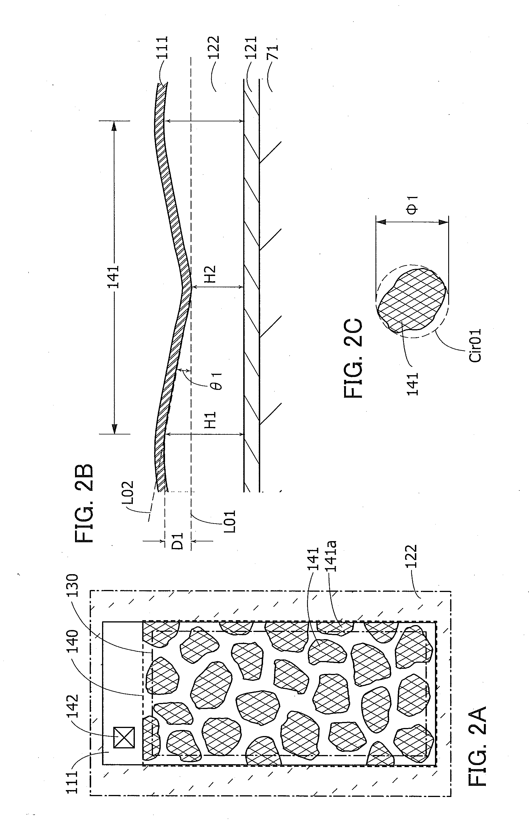
[0128]As described in Embodiments 1 and 2, one of the methods for forming a plurality of depressions in a surface of a reflective electrode is a method of forming a plurality of depressions in a surface of an insulating layer that is a base layer of the reflective electrode. Thus, to increase irregularity of the surface shape of the insulating layer 351 of the EL panel 260, the plurality of depressions 361 with irregular shapes are randomly formed in the surface of the insulating layer 353 (see FIG. 7A).
[0129]However, when the EL panel 260 has a l...
PUM
Abstract
In a light-emitting device where reflective electrodes are regularly arranged, occurrence of interference fringes due to reflection of light reflected by the reflective electrode is inhibited. A surface of the reflective electrode of a light-emitting element is provided with a plurality of depressions. The shapes of the plurality of depressions are different from each other and do not have rotational symmetry. Irregularity of the surface shape of the reflective electrode is increased, which inhibits interference of light reflected by the reflective electrode. To form the plurality of depressions in the surface of the reflective electrode, for example, a surface of an insulating layer that is a base of the reflective electrode is made uneven. Reflecting the surface shape of the insulating layer, the reflective electrode has an uneven surface.
Description
BACKGROUND OF THE INVENTION[0001]1. Field of the Invention[0002]The present invention relates to a light-emitting device including a light-emitting element such as an electroluminescence (EL) element.[0003]2. Description of the Related Art[0004]EL display devices are known as active matrix display devices. A screen of an active matrix EL display device includes a plurality of pixel circuits. Each pixel circuit is provided with an EL element. In the EL display device, the pixel circuit controls the luminance of the EL element so that gray scale display is performed.[0005]In the general structure of an EL element provided in a pixel circuit, a light-emitting layer is provided between a pair of electrodes of an electrode having a light-transmitting property and an electrode having a light-reflecting property. Light generated from the light-emitting layer is reflected by the electrode having a light-reflecting property, passes through the electrode having a light-transmitting property, ...
Claims
Application Information
Patent Timeline
Application Date:The date an application was filed.
Publication Date:The date a patent or application was officially published.
First Publication Date:The earliest publication date of a patent with the same application number.
Issue Date:Publication date of the patent grant document.
PCT Entry Date:The Entry date of PCT National Phase.
Estimated Expiry Date:The statutory expiry date of a patent right according to the Patent Law, and it is the longest term of protection that the patent right can achieve without the termination of the patent right due to other reasons(Term extension factor has been taken into account ).
Invalid Date:Actual expiry date is based on effective date or publication date of legal transaction data of invalid patent.