Display Device

Active Publication Date: 2015-12-17
SEMICON ENERGY LAB CO LTD
View PDF49 Cites 47 Cited by
  • Summary
  • Abstract
  • Description
  • Claims
  • Application Information

AI Technical Summary

Benefits of technology

[0033]One embodiment of the present invention can provide a display device or an input/output device in which irregularity of the surface shape of a black matrix is increased to suppress generation of interference fringes and a reduction in display quality due to reflection of outside light.
[0034]Furthermore, one embodiment of the present invention can provide a display device or an input/output device in which irregularity of the surface shape of a reflective electrode is increased to suppress generation of interference fringes and reflection of images due to reflection of outside light. One embodiment of the present invention can provide a display

Problems solved by technology

Patent Document 1 is expected to be effective to some extent in terms of preventing reflection of images, but there is a problem of a reduction in display quality due to interference fringes because of a dot pattern, which is a highly symmetric planar shape, formed on the surface of a resin

Method used


Image

  • Display Device
  • Display Device
  • Display Device

Examples


embodiment 1

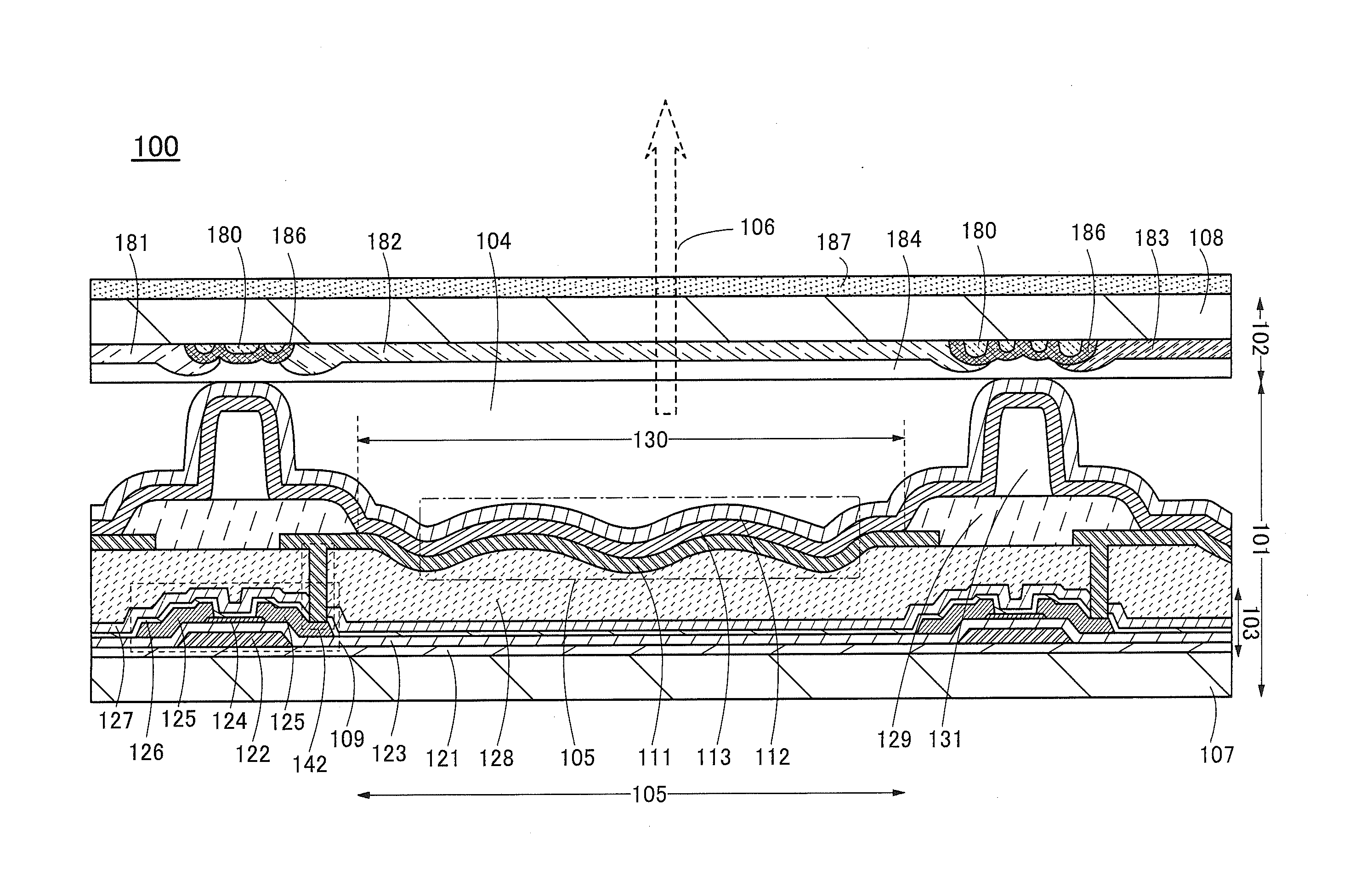
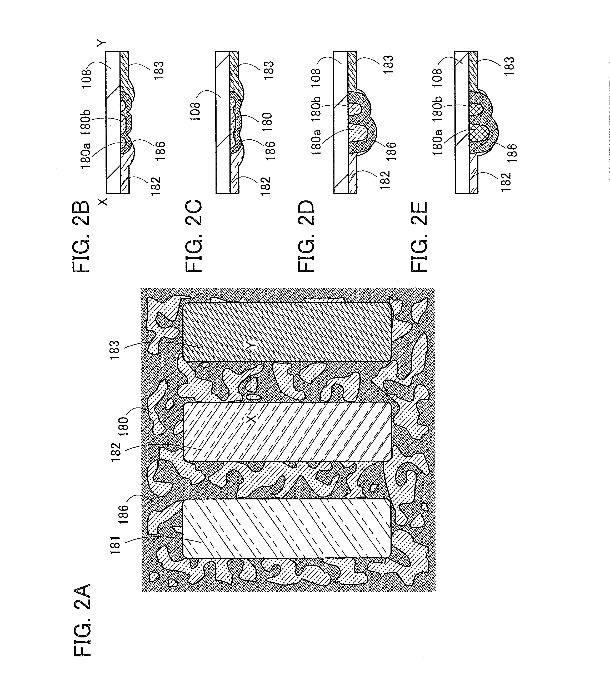
[0069]An EL display device which is an example of one embodiment of the present invention will be described with reference to FIG. 1, FIGS. 2A to 2E, and FIGS. 3A to 3C.

[0070]FIG. 1 is a cross-sectional view showing a structure example of an EL display device 100. The EL display device 100 includes an element substrate 101 and a counter substrate 102. Note that the EL display device 100 has a top-emission structure where light 106 emitted from a light-emitting element 105 is extracted from the counter substrate 102 side.

[Structure Example of Element Substrate]

[0071]The element substrate 101 includes a transistor layer 103 over the substrate 107 and a light-emitting element 105 over the transistor layer 103. The transistor layer 103 includes a transistor, a capacitor, wirings / a group of wirings, and the like which are included in a pixel region and a driver. In FIG. 1, a transistor 109 of a pixel circuit is illustrated as a representative example.

[0072]There is no particular limitati...

embodiment 2

[0138]Embodiment 2 describes a structure of an active matrix EL display device in detail.

[0139]FIG. 4 and FIG. 5 are cross-sectional views each illustrating a structure example of an EL display device. FIG. 20A is a circuit diagram illustrating a configuration example of a pixel circuit. FIG. 20B is a planar layout diagram of the pixel circuit.

[0140]As shown in FIG. 4, an EL display device 260 is similar to the EL display device 100 (FIG. 1) and includes an element substrate 201 and a counter substrate 202. The counter substrate 202 is fixed to the element substrate 201 with a sealant (not illustrated). The EL display device 260 has a top-emission structure like the EL display device 100. A light 200 from a pixel region is emitted from the counter substrate 202 side.

[0141]A light-emitting layer which emits white light is included in a light-emitting element in the pixel region, and the counter substrate 202 is provided with a color filter so that full-color display can be performed....

embodiment 3

[0178]In Embodiment 3, another mode of an active matrix EL display device is described with reference to FIG. 5.

[0179]An EL display device 261 shown in FIG. 5 includes the black matrix 379 and the reflective electrode layer 331. The black matrix 379 has projections, and the reflective electrode layer 331 in the opening 420 does not have a depression. It is difficult to reduce reflection of outside light by the reflective electrode layer 331, but reflection of outside light by the black matrix 379 can be reduced.

[0180]Note that details are omitted because the EL display device 260 is the same as the EL display device 260 in FIG. 4 except for the shape of the insulating layer 353, the reflective electrode layer 331, the light-transmitting conductive layer 334, the light-emitting layer 333, and the semi-transmissive conductive layer 332 in the opening 420.

[0181]This embodiment can be implemented in appropriate combination with any of the structures described in the other embodiments.


PUM


Abstract

Provided is a display device or an input/output device in which reflection of outside light is reduced. The display device includes a first substrate and a second substrate. The first substrate includes a first surface. A transistor is over the first surface. The second substrate includes a second surface. A first structure having a projection, a second structure having a projection, a black matrix covering the first structure and the second structure, and a color filter are over the second surface. The first surface faces the second surface. The black matrix has a plurality of projections reflecting the projection of the first structure and the projection of the second structure. A planar shape of the first structure is different from a planar shape of the second structure.

Description

TECHNICAL FIELD[0001]One embodiment of the present invention relates to a display device or an input / output device. One embodiment of the present invention relates to a display device including a light-emitting element, such as an electroluminescence (EL) element, and a display device including a liquid crystal element.[0002]Note that one embodiment of the present invention disclosed in this specification and the like is not limited to the above technical field and relates to an object, a method, or a manufacturing method. Furthermore, one embodiment of the present invention relates to a process, a machine, manufacture, or a composition of matter. Specific examples of the technical field of one embodiment of the present invention disclosed in this specification include a semiconductor device, a display device, a liquid crystal display device, a light-emitting device, a lighting device, a power storage device, a memory device, an imaging device, an electronic device, an input device,...

Claims


Application Information

Patent Timeline
IPC IPC(8): G02F1/1333H01L27/32H05K1/02G02F1/1368G02F1/1335H01L27/12H01L51/52
CPCG02F1/13338H01L27/124H01L27/1248H01L27/3276H01L27/3248H01L51/5284H05K2201/10166H01L27/3258G02F1/1368G02F1/133345G02F1/133512H05K1/0298H05K2201/10151H01L27/323G02F1/133553G02F1/13394H10K59/40H10K59/124H10K59/12H10K50/813H10K50/822H10K50/865H10K59/38
Inventor JIKUMARU, MIKAKUBOTA, DAISUKEMIYAIRI, NORIKONAGATA, TAKAAKI
Owner SEMICON ENERGY LAB CO LTD
Why Eureka
Try Eureka