Active matrix substrate and display device

a technology of active matrix substrate and substrate, which is applied in the direction of static indicating devices, non-linear optics, instruments, etc., can solve the problem of difficult to reduce the resistance of the frame on the terminal side, and achieve the effect of small resistance change between adjacent signal lines

Active Publication Date: 2015-12-10
SHARP KK
View PDF6 Cites 19 Cited by
  • Summary
  • Abstract
  • Description
  • Claims
  • Application Information

AI Technical Summary

Benefits of technology

[0039]The present invention can provide an active matrix substrate in which a plurality of signal lines are laid with the line pitch becoming narrower, and a change in resistance of two adjacent signal lines is small even if each of the signal lines includes two conductive layers that differ in sheet resistance, and a display device using the active matrix substrate.

Problems solved by technology

However, it is difficult to reduce this frame on the terminal side, since the number of lines is very large compared to the monolithic circuit element.

Method used


Image

  • Active matrix substrate and display device
  • Active matrix substrate and display device
  • Active matrix substrate and display device

Examples


embodiment 1

(Configuration Example of Liquid Crystal Display Device)

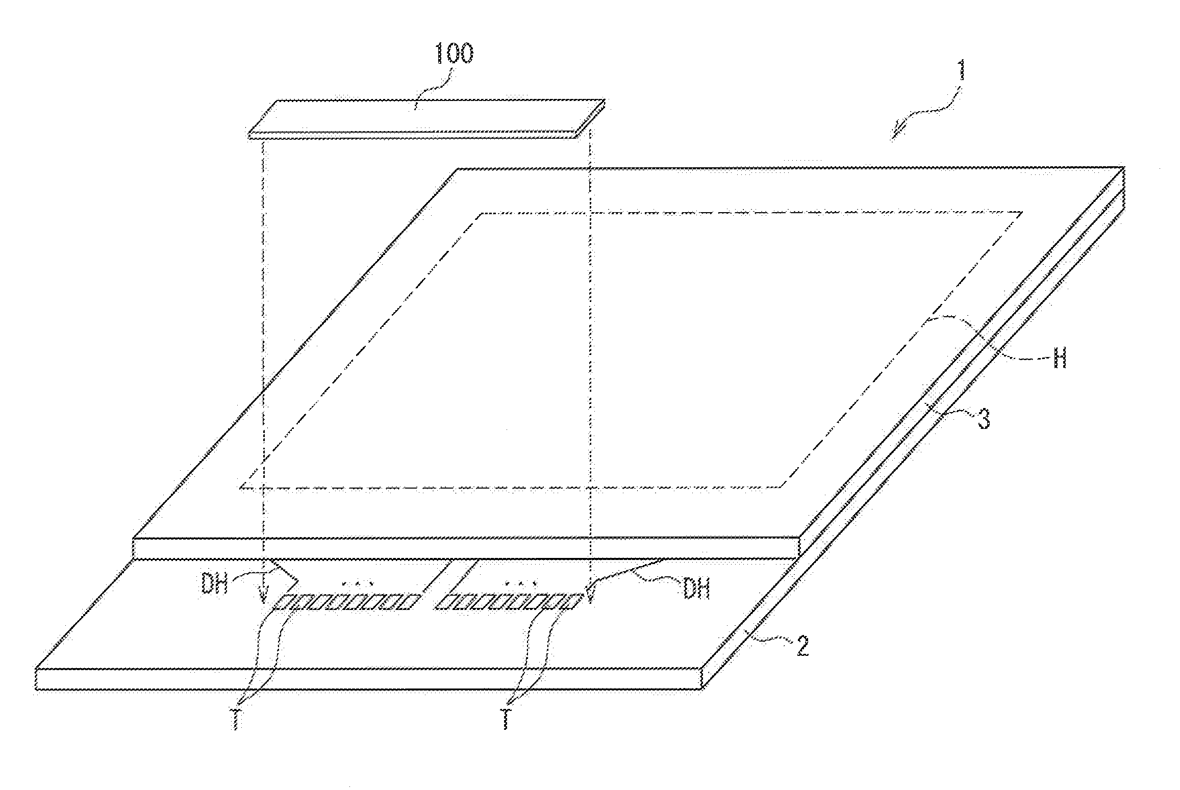
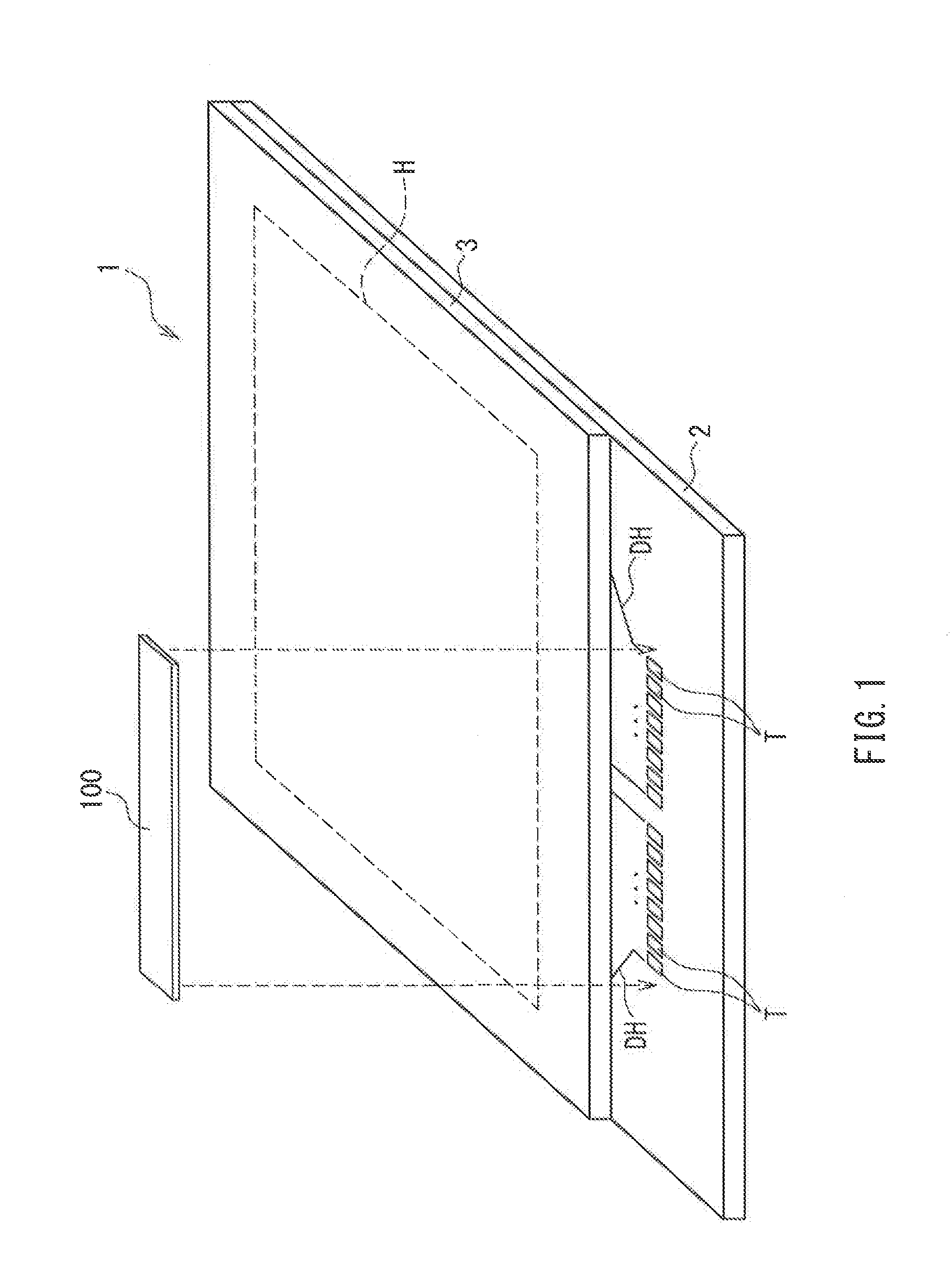
[0064]FIG. 1 is a perspective view of a liquid crystal display device using an active matrix substrate according to Embodiment 1 of the present invention. In FIG. 1, a liquid crystal display device 1 of this embodiment includes an active matrix substrate (TFT substrate) 2 of the present invention and a counter substrate (color filter substrate) 3. The active matrix substrate 2 and the counter substrate 3 are bonded together with a sealing material (as will be described later) so that they face each other. In the liquid crystal display device 1, the sealing material is provided in the form of a frame, and a liquid crystal material is held inside the sealing material to form a liquid crystal layer 18 (see FIG. 7 or 8 as will be described later).

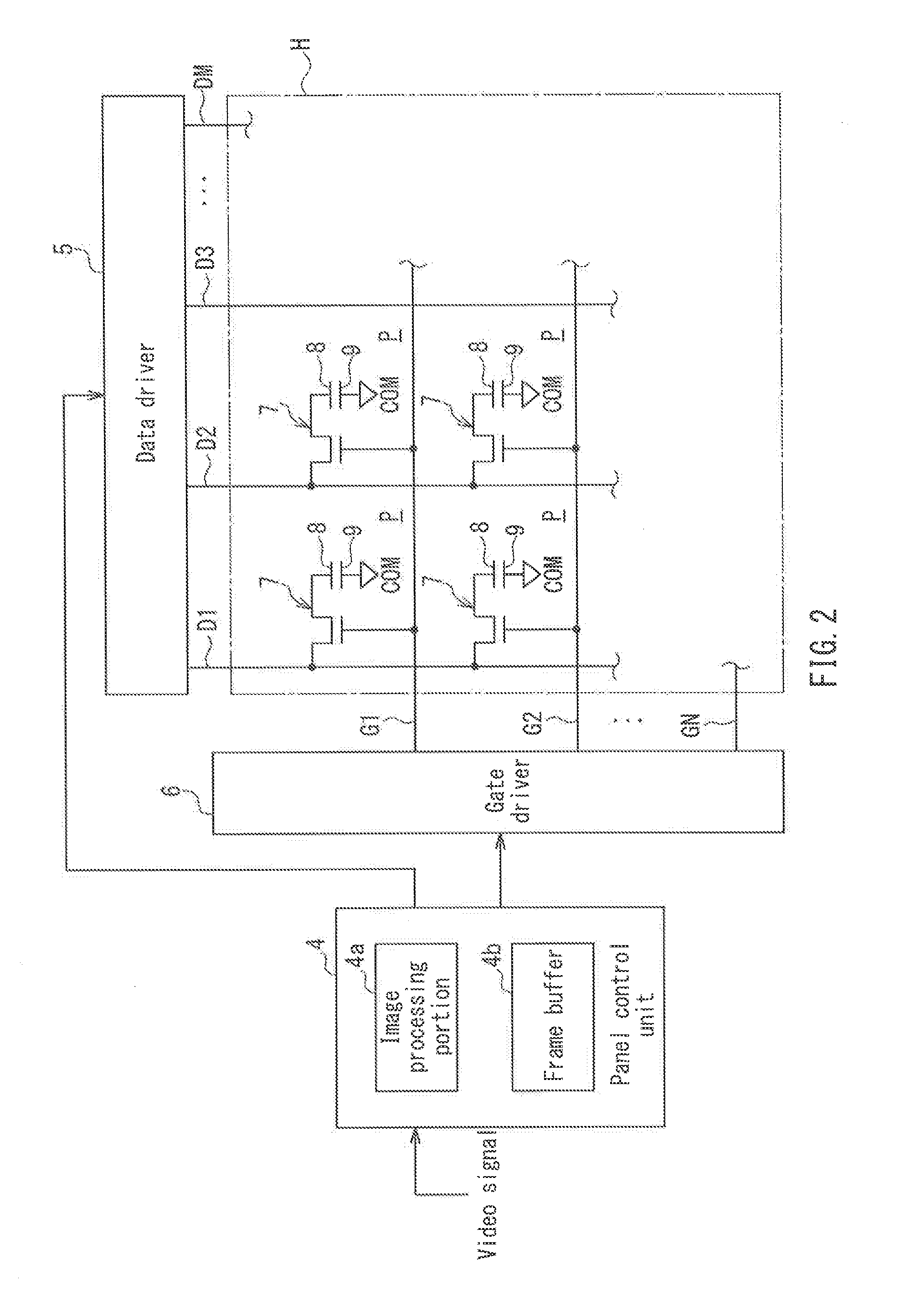
[0065]The liquid crystal display device 1 includes a matrix region H in which a plurality of data lines (source lines) and a plurality of scanning lines (gate lines) are arranged in a matr...

modified example 1

[Modified Example 1]

[0282]FIG. 20 is a plan view for explaining the layout and wiring structure of the video signal lines in the active matrix substrate.

[0283]In FIG. 20, Modified Example 1 mainly differs from Embodiment 1 in the following point. There are five pairs of line groups, in each of which two line groups are symmetrical with respect to the Y axis, and the conductive layers of the first and second line portions of one line group are different from those of the first and second line portions of the other line group. The same components as those of Embodiment 1 are denoted by the same reference numerals, and the explanation will not be repeated.

[0284]In the active matrix substrate 2 of Modified Example 1, the first line group A, the second line group B, the third line group C, the fourth line group D, the fifth line group E, the sixth line group E′y, the seventh line group D′y, the eighth line group C′y, the ninth line group B′y, and the tenth line group A′y are arranged in ...

modified example 2

[Modified Example 2]

[0290]FIG. 21 is a plan view for explaining the layout and wiring structure of the video signal lines in the active matrix substrate.

[0291]In FIG. 21, Modified Example 2 mainly differs from Embodiment 1 in the following point. The fourth and fifth line groups and their corresponding line groups are removed, and three pairs of line groups, in each of which two line groups are symmetrical with respect to the Y axis, are provided. The same components as those of Embodiment 1 are denoted by the same reference numerals, and the explanation will not be repeated.

[0292]In the active matrix substrate 2 of Modified Example 2, the first line group A, the second line group B, the third line group C, the eighth line group C′y, the ninth line group B′y, and the tenth line group A′y are arranged in this order when seen from the left side of the sheet of FIG. 21.

[0293]As described above, the line group without the letter y such as “the first line group A” and the line group with...


PUM


Abstract

An active matrix substrate includes a plurality of signal lines, each of which includes first and second line portions and an inner connection portion (connection portion) that connects the first and second line portions. The first and second line portions of one of two adjacent signal lines are made of first and second conductive layers, respectively, and the first and second line portions of the other of the two adjacent signal lines are made of second and first conductive layers, respectively. The position of the connection portion of each of the signal lines is determined in accordance with the layout position of that signal line in the line region.

Description

TECHNICAL FIELD[0001]The present invention relates to an active matrix substrate including a plurality of data lines and a plurality of scanning lines that are arranged in a matrix, and a display device using the active matrix substrate.BACKGROUND ART[0002]In recent years, e.g., a liquid crystal display device has been widely used for electrical equipment, including a liquid crystal television, a monitor, a portable telephone, a digital camera, and an information terminal, as a flat panel display (display cell) having features such as small thickness and light weight compared to a conventional Braun tube. In the liquid crystal display device, it is known to use an active matrix substrate for a liquid crystal panel (display panel). The active matrix substrate includes the following: a plurality of data lines (source lines) and a plurality of gate lines (scanning lines) that are arranged in a matrix; switching elements such as thin film transistors (TFTs) that are provided in the vici...

Claims


Application Information

Patent Timeline
Patent Type & Authority Applications(United States)
IPC IPC(8): G09G3/36
CPCG09G2310/0202G09G3/3648G02F1/1345G02F1/13452G02F1/136286
Inventor FUJIKAWA, YOHSUKE
Owner SHARP KK
Why Eureka
Try Eureka