Electronic device having a hidden input key and method of manufacturing an electronic device

a technology of electronic devices and input keys, which is applied in the direction of pulse techniques, electrical apparatus casings/cabinets/drawers, instruments, etc., can solve the problems of difficult detection, or inability to detect at all, and achieve the effect of reducing the tactile response of the key, changing the electrical characteristic such as resistance or capacitance, and reducing the change of the electrical characteristi

Inactive Publication Date: 2014-02-04
SONY CORP +1
View PDF10 Cites 17 Cited by
  • Summary
  • Abstract
  • Description
  • Claims
  • Application Information

AI Technical Summary

Benefits of technology

[0018]An end of the conductive material may be flush with the outer face of the housing. This reduces the tactile response of the key upon contact with a user's skin. Alternatively, an end of the conductive material may also protrude from the outer face.
[0019]The key may be configured such that it includes a plurality of micro holes in which a conductive material is respectively arranged so as to extend from the inner face to the outer face of a wall of the housing. The plurality of micro holes associated with a key may be arranged in an array. The plurality of micro holes having a conductive material extending therein may be configured in an identical manner, but may have different orientations of their centre axes. Thereby, the active area in which a user can actuate the key by bringing his / her finger into contact with the outer face of the housing may be enlarged to a desired size. Further, the change in the electrical characteristic, such as resistance or capacitance, occurring upon engagement and disengagement of the user's skin with the outer face of the housing may be increased.

Problems solved by technology

The micro hole may be dimensioned such that it is difficult to detect, or cannot be detected at all, by an unaided human eye of an adult human having average sight.

Method used


Image

  • Electronic device having a hidden input key and method of manufacturing an electronic device
  • Electronic device having a hidden input key and method of manufacturing an electronic device
  • Electronic device having a hidden input key and method of manufacturing an electronic device

Examples


Embodiment Construction

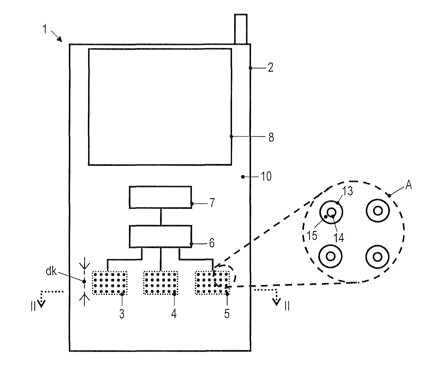
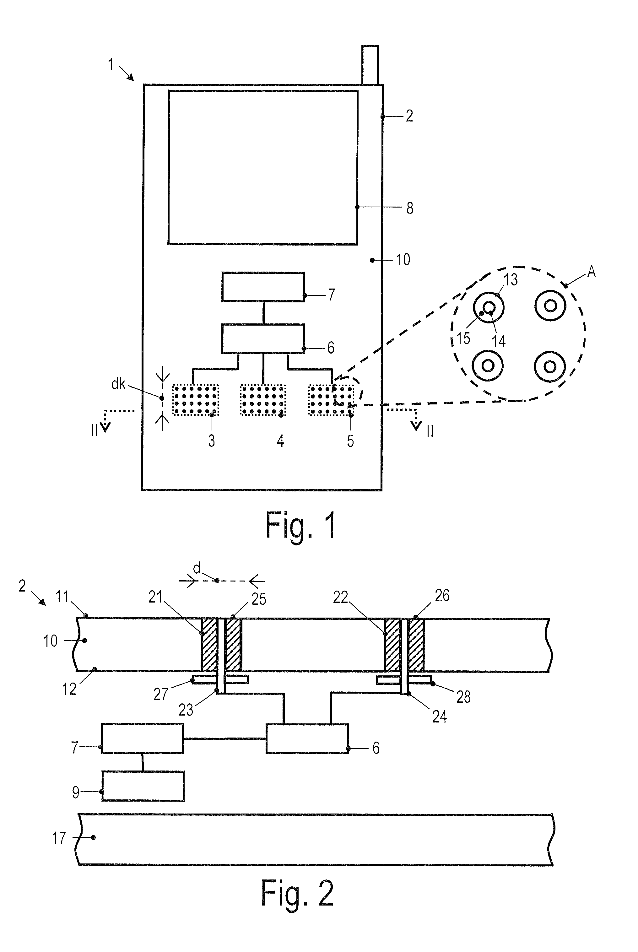
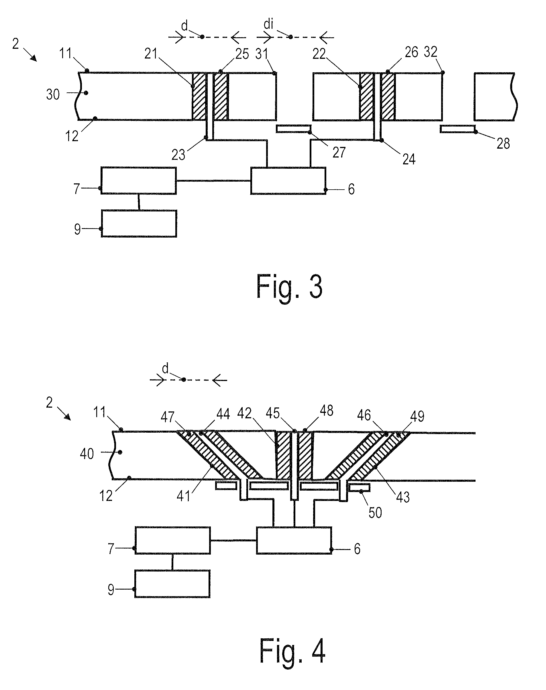
[0041]In the following, embodiments of the present invention will be described in detail with reference to the accompanying drawings. It is to be understood that the following description of embodiments is not to be taken in a limiting sense. The scope of the invention is not intended to be limited by the embodiments described hereinafter or by the drawings, which are taken to be illustrative only. Rather, the scope of the invention is intended to be defined only by the appended claims and equivalents thereof.

[0042]It is to be understood that the drawings are to be regarded as being schematic representations only, and elements illustrated in the drawings are not necessarily shown to scale. Rather, the various elements are represented such that their function and general purpose become apparent to a person skilled in the art.

[0043]It is also to be understood that, in the following description of exemplary embodiments, any direct connection or coupling between functional blocks, devic...


PUM

PropertyMeasurementUnit
angleaaaaaaaaaa
distanceaaaaaaaaaa
distanceaaaaaaaaaa

Abstract

An electronic device comprises a housing having an outer face and an inner face. A key is provided on the housing, which comprises a micro hole formed in the housing and a conductive material extending within the micro hole to the outer face of the housing. A sensor is coupled to the conductive material to detect whether an object is brought into contact or out of contact with the micro hole at the outer face.

Description

[0001]The invention relates to an electronic device and a method of manufacturing the same. The invention relates in particular to such a device having an input key to allow a user to input data or to control operation of the electronic device.BACKGROUND OF THE INVENTION[0002]Electronic devices, such as portable electronic devices, frequently comprise a user interface that allows a user to enter control commands or other data. Many conventional user interfaces which have been used for several decades involve hardware keys which include mechanically moveable elements. With a view to device aesthetics, there have been attempts to change the construction of electronic devices, and in particular of portable electronic devices, so as to reduce the number of mechanically moveable elements which are provided on the electronic device. One route which has been pursued has been to utilize touch sensitive screens. Such touch sensitive screens may traditionally be based on resistive or capaciti...

Claims


Application Information

Patent Timeline
Patent Type & Authority Patents(United States)
IPC IPC(8): H03K17/975
CPCG06F3/0202H03K17/9645H05K1/0275H05K1/053H05K1/115H05K1/116H05K1/162H05K1/167H05K3/0026H05K3/4015H05K3/4046H05K3/445H05K2201/0108H05K2201/0376H05K2201/09545H05K2201/09609H05K2201/09836H05K2201/0999H05K2201/10121H05K2201/10151H05K2203/107Y10T29/49002
Inventor MORAN, JONASKLEVERMAN, MATS
Owner SONY CORP
Why Eureka
Try Eureka