Substrate-mounted circuit module having components in a plurality of contacting planes

a circuit module and substrate technology, applied in the field of circuit modules, can solve problems such as long printed circuit traces, achieve the effects of reducing reactive power, improving electromagnetic compatibility, and reducing space requirements

Inactive Publication Date: 2011-05-05
ROBERT BOSCH GMBH
View PDF18 Cites 20 Cited by
  • Summary
  • Abstract
  • Description
  • Claims
  • Application Information

AI Technical Summary

Benefits of technology

[0008]The circuit module according to the present invention, as well as the production method according to the present invention, enable the positioning of components having improved electromagnetic compatibility, reduced reactive power and reduced space requirement. The present invention enables a compact construction while employing usual cost-effective substrates, which are able to be processed using extensively known processing technologies. When using the present invention, while employing usual substrates, one is able to provide an additional contact plane which clearly simplifies the wiring by printed circuit traces. The reduced complexity leads to a reduced reactive power and to a saving in wiring surface. In addition, the present invention leads to improved heat dissipation of power components that are connected according to the present invention. The carrier layer is used as a mechanical / electrical contacting plane as well as a heat sink / heat dissipation. In addition, bonds and other connections are saved which are provided in addition to the printed circuit traces. The components, as well as the associated terminals of the circuit module, according to the present invention, are able to be positioned at greater degrees of freedom and higher flexibility compared to the related art. In addition, the present invention makes possible a combination of power current applications and control applications on the same substrate. In other words, power components are able to be positioned together with control components or logic components on the same substrate. This additionally increases the integration density. Furthermore, the present invention enables the production of contacts between components and the substrate via a low-temperature sintering connection, such a connection leading to an increased resistance to temperature changes.

Problems solved by technology

However, in more complex circuits, for instance, in three-phase rectifier bridges, long printed circuit traces come about, since only the uppermost layer, that is, the wiring layer provided on the insulating layer, which provides printed circuit traces, is used for connecting the components.

Method used


Image

  • Substrate-mounted circuit module having components in a plurality of contacting planes
  • Substrate-mounted circuit module having components in a plurality of contacting planes

Examples


Embodiment Construction

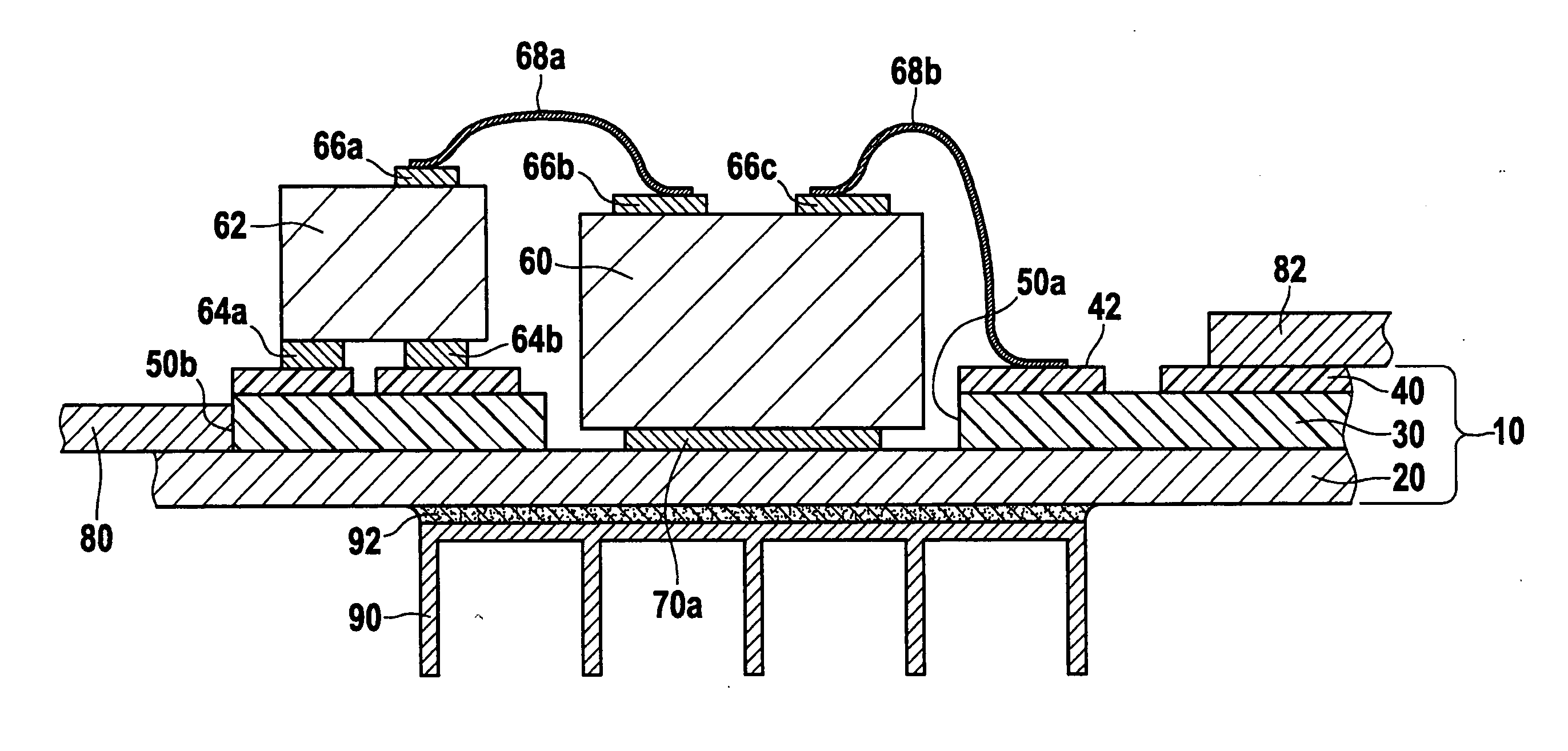
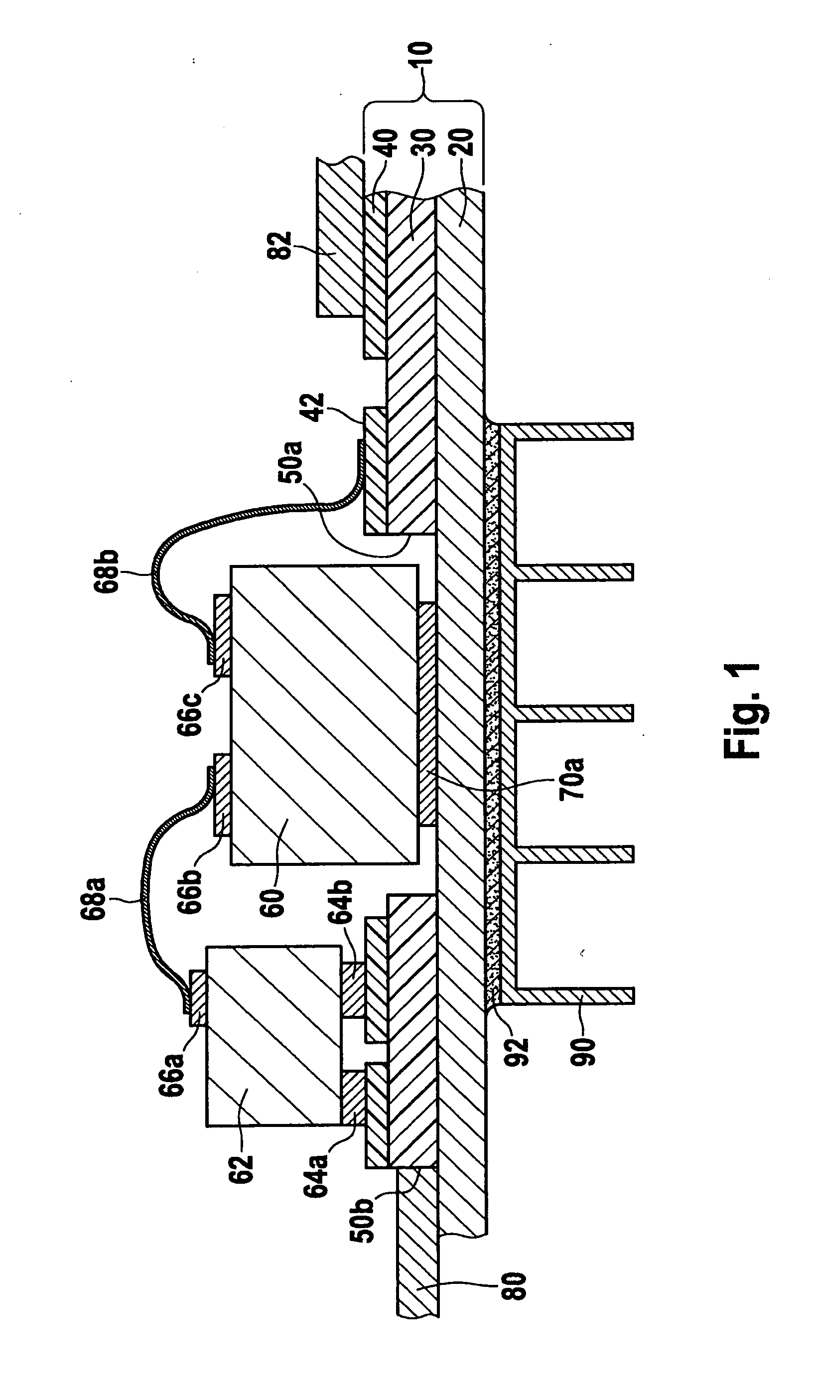
[0025]FIG. 1 shows a circuit module having a substrate 10, which provides a carrier layer 20 provided to be made of metal, an electrically insulating insulating layer 30 and an electrically conducting wiring layer 40, printed circuit traces by patterning and / or pads and electrical contact surfaces (not shown). Carrier layer 20 is continuous, whereas insulating layer 30, lying over it, has a first recess 50a according to the present invention, in which the first surface of carrier layer 20 is exposed and a component 60 is in electrical contact with carrier layer 20 via contact elements 70a. A second recess 50b also provides an exposed contact surface of the first surface of carrier layer 20, in section 50b a sheet metal section 80 having been pressed onto carrier layer 20. Sheet metal section 80 was a punch grid during the production process, and was separated from the rest of the punch grid during production, especially from a blanking frame. Wiring layer 40 also has interruptions, ...


PUM

PropertyMeasurementUnit
electrically conductingaaaaaaaaaa
electricalaaaaaaaaaa
heat-conductingaaaaaaaaaa

Abstract

In a circuit module having components that are fastened to a substrate, the substrate includes a carrier layer made of metal and having a first surface, a first insulating layer bordering directly on the carrier layer being situated on the first surface. The substrate also includes a first wiring layer bordering directly on the first insulating layer, which conducts electrically and is situated on the first insulating layer. The substrate includes a first contact plane, which runs along the first surface, at least one of the components being directly connected electrically to the carrier layer in the first contact plane.

Description

BACKGROUND OF THE INVENTION[0001]1. FIELD OF THE INVENTION[0002]The present invention relates to a circuit module in which electronic components fastened on the surface are fastened on a substrate.[0003]2. DESCRIPTION OF RELATED ART[0004]Such a fastening structure is known from the field of surface-mounted components (surface-mounted technology SMT).[0005]Published German patent application document DE 100 38 092 A1 describes an electrical module in which a chip is connected to a cooling body, an IMS substrate providing printed circuit traces to which the chip is connected. A metallic base plate, which forms the carrier of the substrate, it is true, is used for thermal connection as well as for mechanical stabilization, but is separated from the chip via an insulating layer. Consequently, this document shows a connecting structure based exclusively on printed circuit traces, which is separated from the metallic carrier plate of the substrate by an insulating layer. In the same way, ...

Claims


Application Information

Patent Timeline
Patent Type & Authority Applications(United States)
IPC IPC(8): H05K1/18H05K1/05H01K3/10
CPCH01L23/3677Y10T29/49162H01L24/49H01L25/072H01L2224/32225H01L2224/45124H01L2224/45144H01L2224/48091H01L2224/48137H01L2224/48227H01L2224/49H01L2924/01005H01L2924/01013H01L2924/01029H01L2924/01033H01L2924/01042H01L2924/0105H01L2924/01052H01L2924/01079H01L2924/01082H01L2924/13055H01L2924/13091H01L2924/19041H01L2924/30107H01L24/45H01L2924/13033H01L2924/13034H01L2924/1301H01L2924/12041H01L2224/73265H01L2224/48472H01L2924/01014H01L2924/014H01L2924/01006H01L24/48H01L2924/00014H01L2924/00H01L23/142H01L2224/45015H01L2924/14H01L2924/181
Inventor KIMMICH, PETERNGUYEN, QUOC-DAT
Owner ROBERT BOSCH GMBH
Why Eureka
Try Eureka