Finfet devices having asymmetrical epitaxially-grown source and drain regions and methods of forming the same
a technology of asymmetric source and drain region, which is applied in the direction of semiconductor devices, electrical devices, transistors, etc., can solve the problems of reducing reducing the size of the distance between the fins, and avoiding the merger of epitaxially grown source and drain regions of adjacent fins
- Summary
- Abstract
- Description
- Claims
- Application Information
AI Technical Summary
Problems solved by technology
Method used
Image

Examples
Embodiment Construction
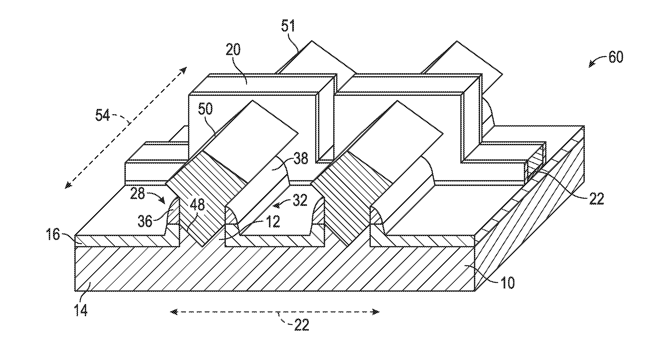
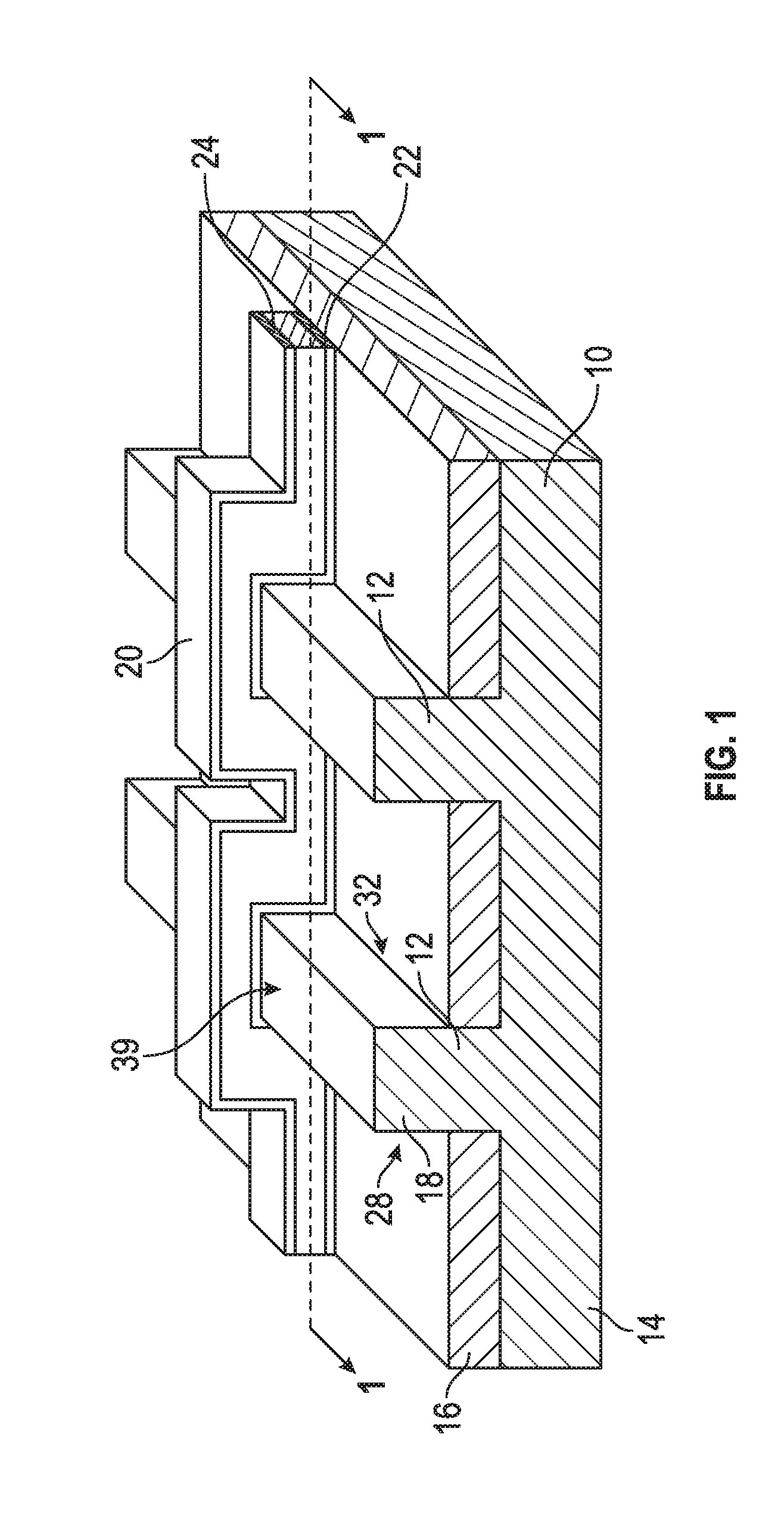
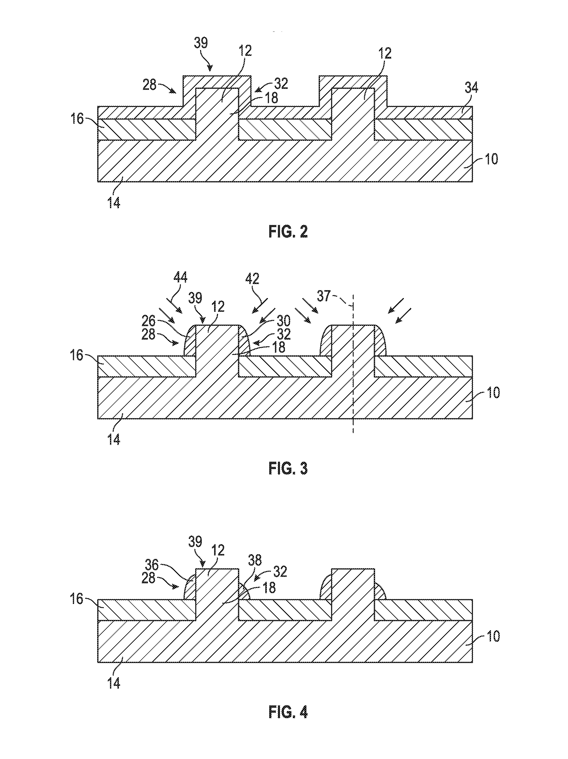
[0015]The following detailed description is merely exemplary in nature and is not intended to limit the fin field-effect transistor (FinFET) devices and methods of forming the FinFET devices as contemplated herein. Furthermore, there is no intention to be bound by any theory presented in the preceding background or the following detailed description.
[0016]Embodiments of the present disclosure are generally directed to FinFET devices and methods for forming the same. For the sake of brevity, conventional techniques related to FinFET device fabrication may not be described in detail herein. Moreover, the various tasks and process steps described herein may be incorporated into a more comprehensive procedure or process having additional steps or functionality not described in detail herein. In particular, various steps in the manufacture of semiconductor-based transistors are well-known and so, in the interest of brevity, many conventional steps will only be mentioned briefly herein or...
PUM
 Abstract
Description
Claims
Application Information
 - R&D Engineer
- R&D Manager
- IP Professional
- Industry Leading Data Capabilities
- Powerful AI technology
- Patent DNA Extraction
Browse by: Latest US Patents, China's latest patents, Technical Efficacy Thesaurus, Application Domain, Technology Topic.
© 2024 PatSnap. All rights reserved.Legal|Privacy policy|Modern Slavery Act Transparency Statement|Sitemap