Memory device and fabricating method thereof

a memory device and memory technology, applied in the field of memory devices, can solve the problems of insufficient device performance of such dram in advanced applications of technology

Active Publication Date: 2017-03-09
MICRON TECH INC
View PDF0 Cites 10 Cited by
  • Summary
  • Abstract
  • Description
  • Claims
  • Application Information

AI Technical Summary

Benefits of technology

[0067]The embodiments of the present disclosure discussed above have advantages over existing memory devices and processes, and the advantages are summarized below. The memory device of the present disclosure is a novel structure, which apples the void as the cap for the gate structure to replace the dielectric material used in general structure. As a result, the electrical potential coupling between the active regions can be effectively reduced, and lower electrical potential can get cell junction electrical and GIDL improvement. Further, the void with gaseous material provided better stress relax function than general structure filled with solid material. Accordingly, the performance of the memory device can be improved.

Problems solved by technology

However, as the transistor size is reduced, the device performance of such DRAM is still not satisfactory in advanced applications of technology.

Method used


Image

  • Memory device and fabricating method thereof
  • Memory device and fabricating method thereof
  • Memory device and fabricating method thereof

Examples


Embodiment Construction

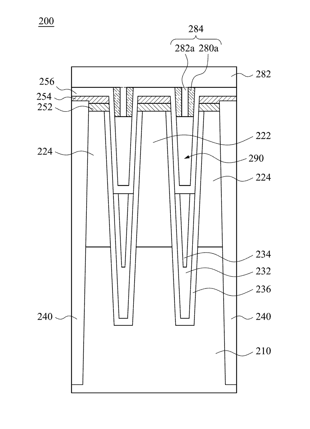
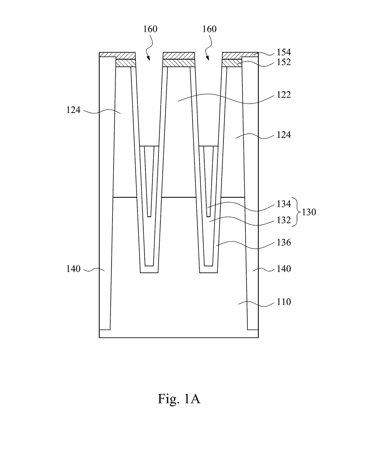
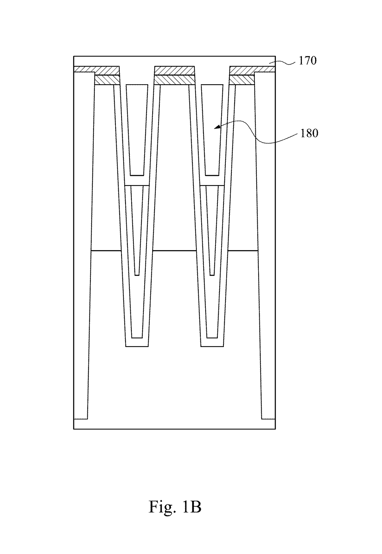
[0028]Reference will now be made in detail to the present embodiments of the invention, examples of which are illustrated in the accompanying drawings. Wherever possible, the same reference numbers are used in the drawings and the description to refer to the same or like parts.

[0029]The following embodiments are disclosed with accompanying diagrams for detailed description. For illustration clarity, many details of practice are explained in the following descriptions. However, it should be understood that these details of practice do not intend to limit the present invention. That is, these details of practice are not necessary in parts of embodiments of the present invention. Furthermore, for simplifying the drawings, some of the conventional structures and elements are shown with schematic illustrations.

[0030]As aforementioned problems, requirements in a memory device are becoming more challenging. For instance, the voltage difference between different active regions of a memory d...


PUM


Abstract

A memory device and a method for fabricating the same are provided. The memory device includes a substrate, a first active region, a second active region, a gate structure, and a capping layer. The first active region and the second active region are alternately disposed in the substrate. The gate structure is disposed in the substrate and between the first active region and the second active region. The capping layer is over the gate structure to define a void therebetween.

Description

BACKGROUNDDescription of Related Art[0001]A Dynamic Random Access Memory (DRAM) is an essential element in many electronic products. To increase component density and improve overall performance of DRAM, industrial manufacturers make constant efforts to reduce the sizes of transistors for the DRAM. However, as the transistor size is reduced, the device performance of such DRAM is still not satisfactory in advanced applications of technology.[0002]Accordingly, an improved memory device and a fabricating method thereof are required.SUMMARY[0003]An aspect of the present disclosure provides a memory device. The memory device includes a substrate, a first active region, a second active region, a gate structure, and capping layer. The first active region and the second active region are alternately disposed in the substrate. The gate structure is disposed in the substrate and between the first active region and the second active region. The capping layer is over the gate structure to defi...

Claims


Application Information

Patent Timeline
Patent Type & Authority Applications(United States)
IPC IPC(8): H01L27/108H01L29/49
CPCH01L27/10876H01L27/10823H10B12/37H10B12/01H10B12/00H10B12/30H01L28/00H10B12/34H10B12/053H10B43/27
Inventor WU, TIEH-CHIANG
Owner MICRON TECH INC
Why Eureka
Try Eureka