Semiconductor module

a technology of semiconductor modules and membranes, applied in the direction of semiconductor devices, semiconductor/solid-state device details, electrical apparatus, etc., can solve problems such as degrading insulation properties, achieve the effects of preventing or reducing the generation of excessive pressure inside the sealing gel, preventing or reducing the application of excessive stress, and improving the reliability of the semiconductor modul

Active Publication Date: 2017-11-30
MITSUBISHI ELECTRIC CORP
View PDF3 Cites 1 Cited by
  • Summary
  • Abstract
  • Description
  • Claims
  • Application Information

AI Technical Summary

Benefits of technology

[0011]The first semiconductor module according to the present invention is configured such that the sealing-gel-expansion suppressing plate is placed to be inclined to the upper surface of the sealing gel to thus prevent or reduce the generation of an excessive pressure inside the sealing gel when the sealing gel expands. In other words, such placement prevents or reduces the application of an excessive stress to the sealed object. Additionally, the placement of the sealing-gel-expansion suppressing plate prevents the sealing gel from being detached from the sealed object. This improves the reliability of the semiconductor module.
[0012]The second semiconductor module according to the present invention is configured such that a region in which the height of the upper surface of the sealing gel is relatively low includes a space that allows the sealing gel to expand upward between the sealing-gel-expansion suppressing plate and the upper surface. Consequently, if the sealing gel expands, the excessive stress on the sealed object would be reduced. Additionally, when the sealing gel further expands to reach the sealing-gel-expansion suppressing plate, the sealing-gel-expansion suppressing plate suppresses the expansion of the sealing gel. This prevents the sealing gel from being detached from, for instance, the insulating substrate. This improves the reliability of the semiconductor module.
[0013]The third semiconductor module according to the present invention is configured such that when the sealing gel starts to expand, the buffer material slightly suppresses the expansion at first. This prevents or reduces the excessive stress on the sealed object. When the sealing gel further expands, the sealing-gel-expansion suppressing plate suppresses the expansion of the sealing gel. This prevents the sealing gel from being detached from the sealed object. This improves the reliability of the semiconductor module.
[0014]The fourth semiconductor module according to the present invention is configured such that if the sealing gel expands, spaces of the plurality of holes would absorb the expansion. This prevents or reduces the excessive stress on the sealed object. When the sealing gel further expands, the sealing-gel-expansion suppressing plate suppresses the expansion of the sealing gel. This prevents the sealing gel from being detached from the sealed object. This improves the reliability of the semiconductor module.

Problems solved by technology

Moisture absorption of the sealing gel and temperature change during the operation of semiconductor module can cause the sealing gel to expand and contract to thus cause damage, such as a broken wire, to a sealed object.
Additionally, the sealing gel is detached from, for instance, the insulating substrate to thus degrade insulation properties.

Method used


Image

  • Semiconductor module
  • Semiconductor module
  • Semiconductor module

Examples


first embodiment

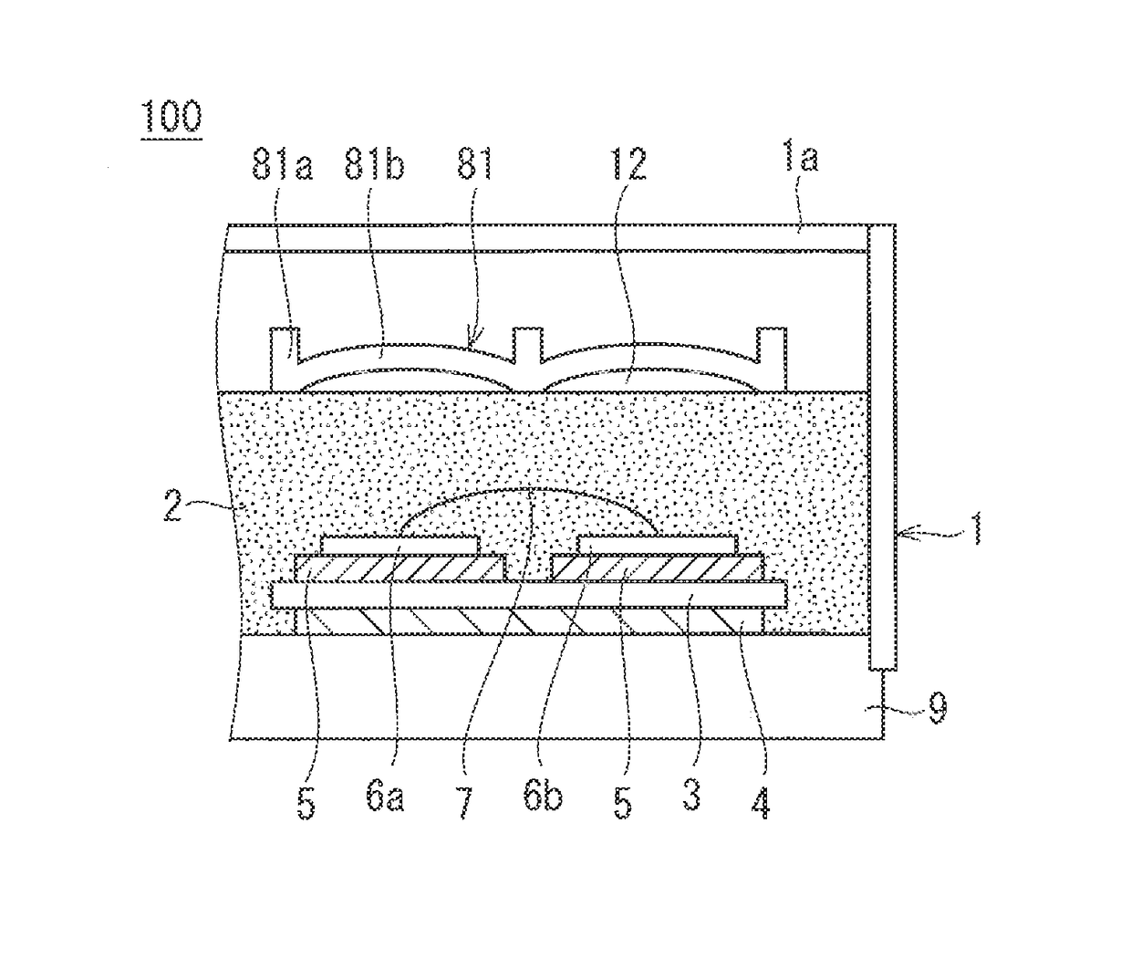
[0035]FIG. 1 is a cross-sectional view of a semiconductor module 100 in a first embodiment. FIG. 2 is a plan view of a sealing-gel-expansion suppressing plate 81 in the first embodiment. A description of a configuration of the semiconductor module 100 in the first embodiment, which is the same as the configuration in the prerequisite technique (FIG. 15) except for a sealing-gel-expansion suppressing plate 81, is omitted. It is noted that FIG. 1 is the cross-sectional view taken along the line AA in the plan view FIG. 14) that is used for the prerequisite technique. It is also noted that a cross section taken along the line BB in FIG. 2 corresponds to a cross section of the sealing-gel-expansion suppressing plate 81 in FIG. 1.

[0036]The sealing gel 2 is, for instance, a silicone gel in the first embodiment. The sealing-gel-expansion suppressing plate 81 includes a lattice-shaped frame 81a and an arch 81b that is the inside of the frame 81a, in the first embodiment. As illustrated in F...

second embodiment

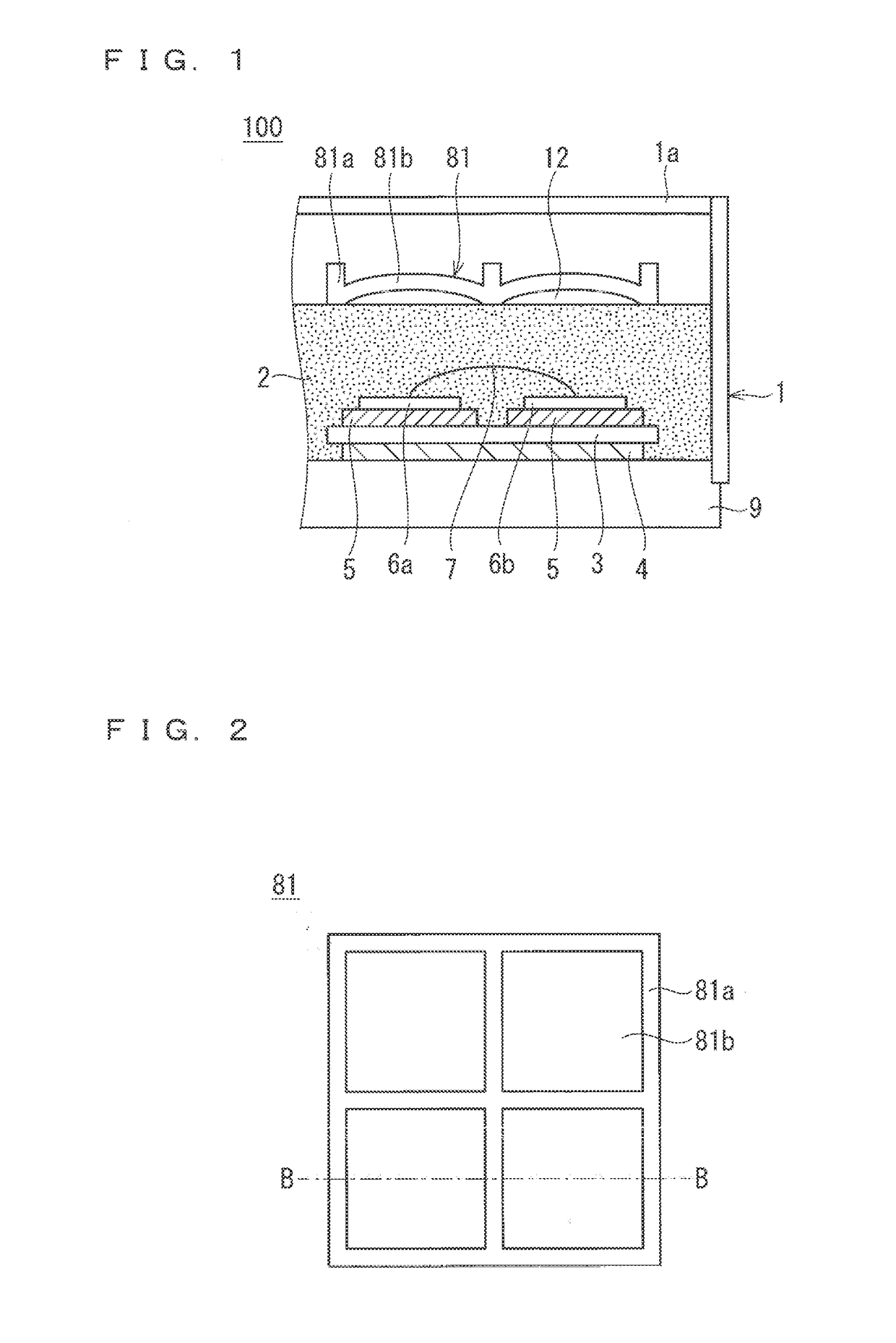
[0047]FIG. 3 is a cross-sectional view of a semiconductor module 200 in a second embodiment. FIG. 4 is a plan view of a sealing-gel-expansion suppressing plate 82 in the second embodiment. A description of a configuration of the semiconductor module 200, which is the same as the configuration in the first embodiment (FIG. 1) except for the sealing-gel-expansion suppressing plate 82, is omitted.

[0048]FIG. 3 is the cross-sectional view taken along the line AA in the plan view (FIG. 14) that is used for the prerequisite technique. Additionally, a cross section in the line CC in FIG. 4 corresponds to a cross section of the sealing-gel-expansion suppressing plate 82 in FIG. 3.

[0049]The sealing-gel-expansion suppressing plate 82 includes first and second sealing-gel-expansion suppressing plates 82a and 82b. As illustrated in FIG. 3, the first and second sealing-gel-expansion suppressing plates 82a and 82b are disposed so that inclined portions 822a and 822b are each inclined to the upper ...

third embodiment

[0053]FIG. 5 is a cross-sectional view of a semiconductor module 300 in a third embodiment. FIG. 6 is a plan view of a sealing-gel-expansion suppressing plate 83 in the third embodiment. A description of a configuration of the semiconductor module 300, which is the same as the configuration in the first embodiment (FIG. 1) except for the sealing-gel-expansion suppressing plate 83, is omitted.

[0054]FIG. 5 is the cross-sectional view taken along the line AA in the plan view (FIG. 14) that is used for the prerequisite technique. Additionally, a cross section in the line DD in FIG. 6 corresponds to a cross section of the sealing-gel-expansion suppressing plate 83 in FIG. 5.

[0055]The sealing-gel-expansion suppressing plate 83 includes first and second sealing-gel-expansion suppressing plates 83a and 83b. As illustrated in FIG. 5, the first and second sealing-gel-expansion suppressing plates 83a and 83b are disposed so that inclined portions 832a and 832b are each inclined to the upper su...


PUM


Abstract

It is an object of the present invention to provide a semiconductor module that reduces an excessive stress on a sealed object due to the expansion and contraction of a sealing gel to thus improve the reliability. A semiconductor module according to the present invention includes: a semiconductor element bonded to a metal pattern on an insulating substrate contained in a case; a sealing gel sealing the insulating substrate and the semiconductor element within the case; and a sealing-gel-expansion suppressing plate disposed in the upper portion of the sealing gel to be at least partially in contact with the sealing gel. The sealing-gel-expansion suppressing plate includes a surface facing the sealing gel and inclined to the upper surface of the sealing gel.

Description

TECHNICAL FIELD[0001]The present invention relates to semiconductor modules, and particularly, to a semiconductor module for an electric power application.BACKGROUND ART[0002]The semiconductor module for the electric power application is typically disposed on an insulating substrate and is typically configured such that a sealing gel seals, within a case, semiconductor elements mutually connected through, for instance, a wire. Moisture absorption of the sealing gel and temperature change during the operation of semiconductor module can cause the sealing gel to expand and contract to thus cause damage, such as a broken wire, to a sealed object. Additionally, the sealing gel is detached from, for instance, the insulating substrate to thus degrade insulation properties.[0003]To solve these problems, Patent Document 1, for instance, describes filling a gel filler into the case before placing a plate to be in close contact with the front surface of the filler. This plate suppresses the s...

Claims


Application Information

Patent Timeline
Patent Type & Authority Applications(United States)
IPC IPC(8): H01L23/24H01L25/07H01L23/532H01L23/28H01L25/18H01L23/14H01L23/528
CPCH01L23/24H01L23/28H01L23/142H01L23/5283H01L25/18H01L23/53228H01L25/07H01L2224/48137H01L23/16H01L23/562
Inventor YASUTOMI, GOROMORISHITA, KAZUHIRODATE, RYUTARO
Owner MITSUBISHI ELECTRIC CORP
Why Eureka
Try Eureka