Semiconductor module
a technology of semiconductor modules and membranes, applied in the direction of semiconductor devices, semiconductor/solid-state device details, electrical apparatus, etc., can solve problems such as degrading insulation properties, achieve the effects of preventing or reducing the generation of excessive pressure inside the sealing gel, preventing or reducing the application of excessive stress, and improving the reliability of the semiconductor modul
- Summary
- Abstract
- Description
- Claims
- Application Information
AI Technical Summary
Benefits of technology
Problems solved by technology
Method used
Image
Examples
first embodiment
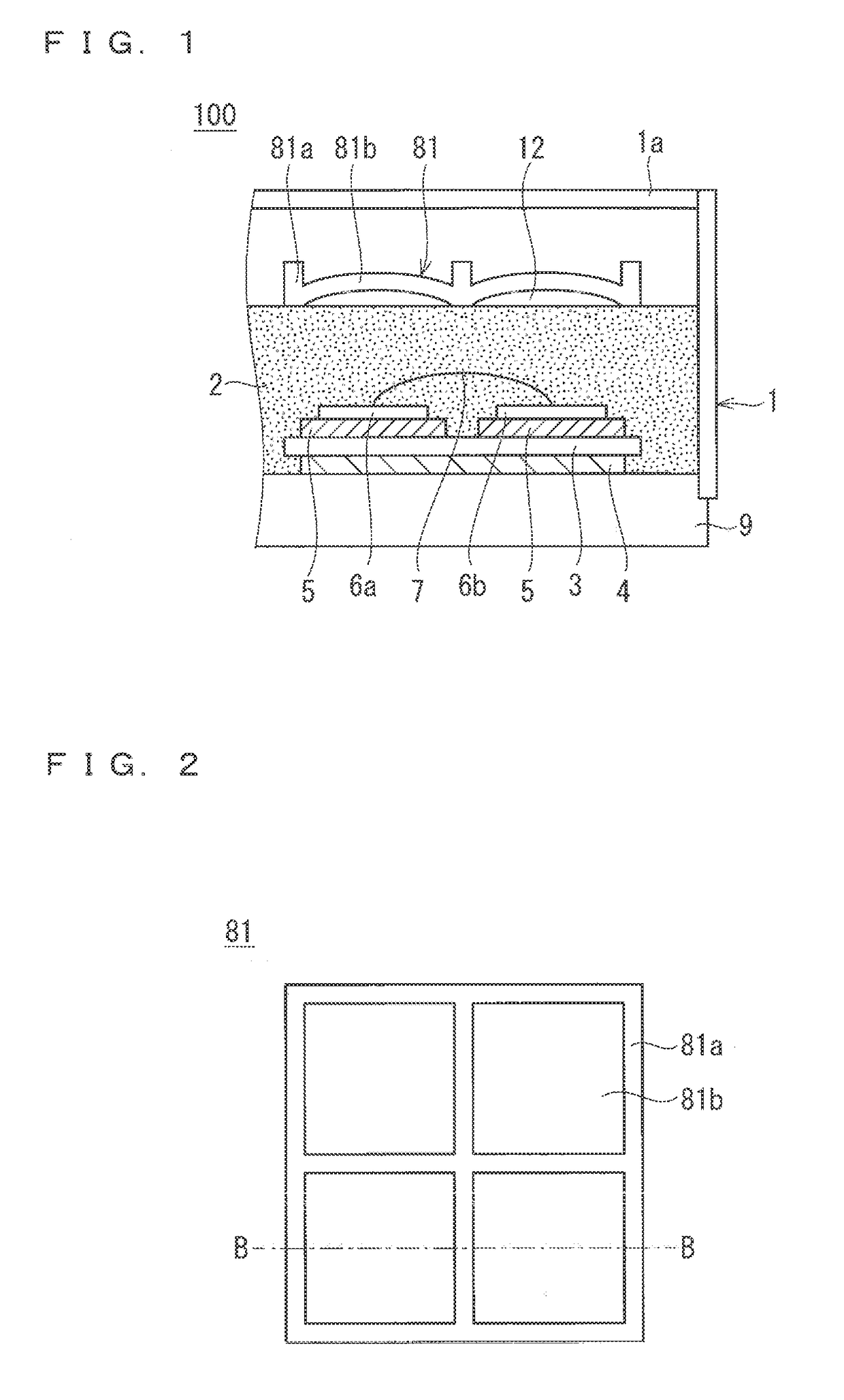
[0040]In the first embodiment, the semiconductor elements 6a and 6b are, for instance, insulated gate bipolar transistor (IGBT) and freewheeling diode connected in parallel. The semiconductor elements 6a and 6b are, for instance, silicon (Si) semiconductor elements, and may be silicon carbide (SiC) semiconductor elements capable of operating under high temperature.
[0041]In the first embodiment, the sealing-gel-expansion suppressing plate 81 may be secured to or in contact with members other than the sealing gel 2. For instance, the sealing-gel-expansion suppressing plate 81 may be secured to the case 1 on its one side (i.e., the side surface of the frame 81a). Alternatively, the frame 81a of the sealing-gel-expansion suppressing plate 81 may extend toward the lid 1a of the case 1 at the top end of the frame 81a to be in contact with or be secured to the lid 1a of the case 1.
[0042]
[0043]The semiconductor module 100 in the first embodiment includes: the semiconductor elements 6a and 6...
second embodiment
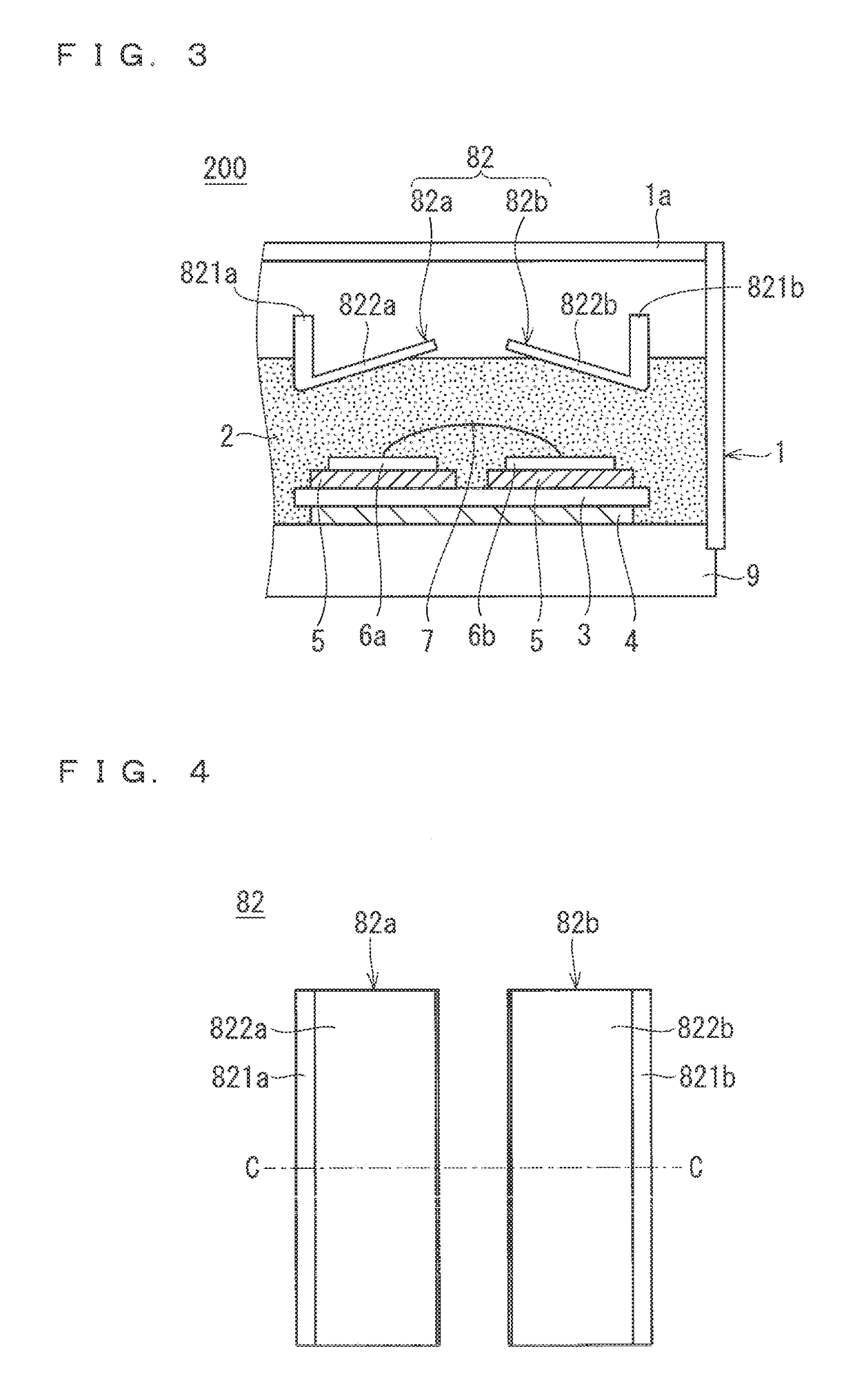
[0056]The semiconductor module 200 in the second embodiment is configured such that the sealing-gel-expansion suppressing plate 82 has an inverted V-shaped cross section.
[0057]Thus, the sealing-gel-expansion suppressing plate 82 is disposed to be inclined to the upper surface of the sealing gel 2 when compared with the corresponding one in the prerequisite technique. Such a configuration prevents or reduces the expansion of the sealing gel 2 more gently than the configuration in the prerequisite technique in which the sealing-gel-expansion suppressing plate 8 is disposed to be horizontal to the upper surface of the sealing gel 2. This prevents or reduces the generation of the excessive pressure inside the sealing gel 2. In other words, this prevents or reduces the application of the excessive stress to the objects, such as the semiconductor elements 6a, 6b, and wire 7, which are sealed by the sealing gel 2. Additionally, providing the sealing-gel-expansion suppressing plate 82 preve...
third embodiment
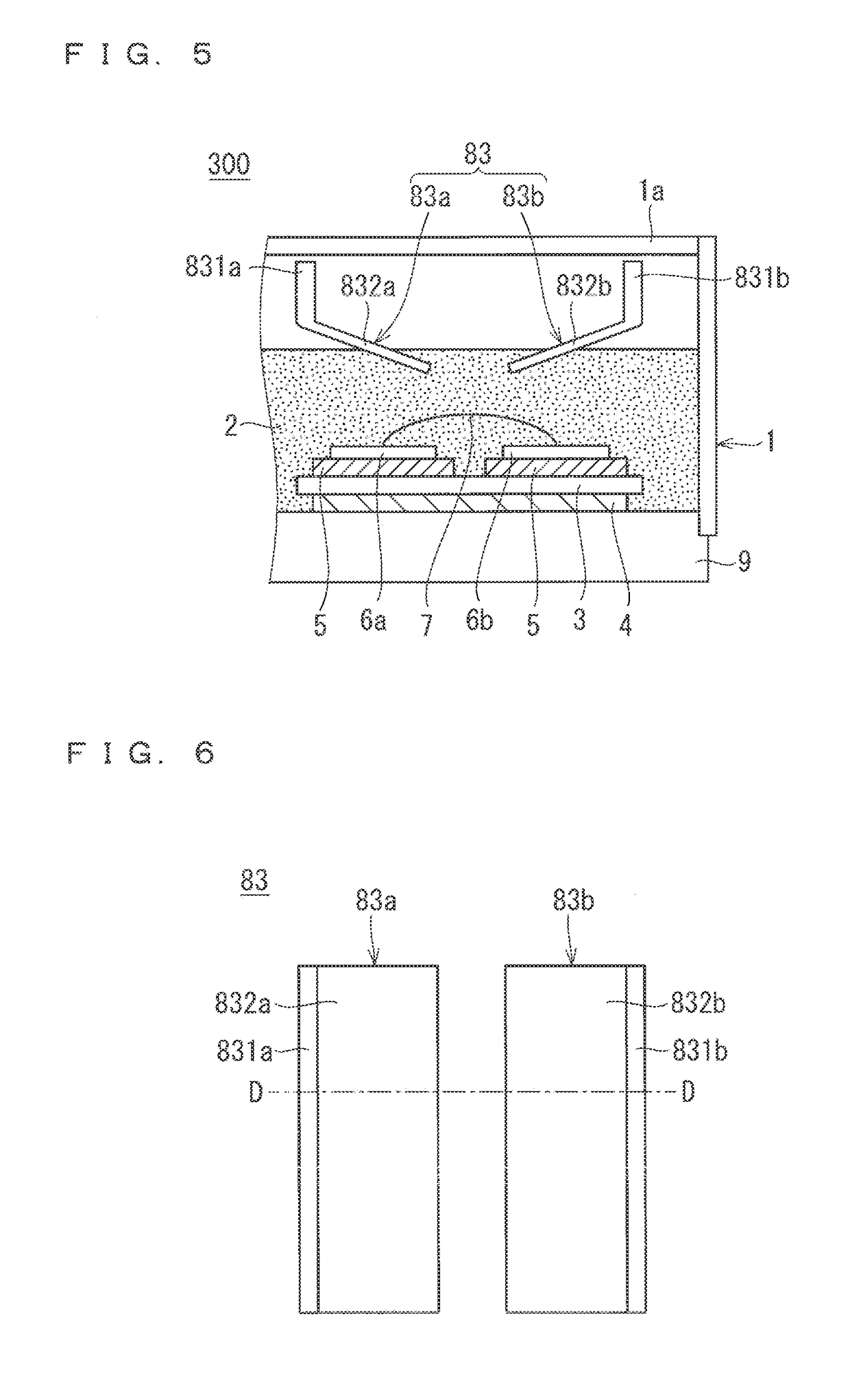
[0064]The semiconductor module 300 in the third embodiment is configured such that the sealing-gel-expansion suppressing plate 83 has a V-shaped cross section.
[0065]Thus, the sealing-gel-expansion suppressing plate 83 is disposed to be inclined to the upper surface of the sealing gel 2 when compared with the corresponding one in the prerequisite technique. Such a configuration prevents or reduces the expansion of the sealing gel 2 more gently than the configuration in the prerequisite technique, in which the sealing-gel-expansion suppressing plate 8 is disposed to be horizontal to the upper surface of the sealing gel 2. This prevents or reduces the generation of the excessive pressure inside the sealing gel 2. In other words, this prevents or reduces the application of the excessive stress to the semiconductor element 6a, 6b and wire 7, which are sealed by the sealing gel 2. Additionally, providing the sealing-gel-expansion suppressing plate 83 prevents the sealing gel 2 from being ...
PUM
 Abstract
Description
Claims
Application Information
 - R&D
- Intellectual Property
- Life Sciences
- Materials
- Tech Scout
- Unparalleled Data Quality
- Higher Quality Content
- 60% Fewer Hallucinations
Browse by: Latest US Patents, China's latest patents, Technical Efficacy Thesaurus, Application Domain, Technology Topic, Popular Technical Reports.
© 2025 PatSnap. All rights reserved.Legal|Privacy policy|Modern Slavery Act Transparency Statement|Sitemap|About US| Contact US: help@patsnap.com


