Flexible Array Substrate, the Preparation Method Thereof, and Flexible Display Device

Inactive Publication Date: 2018-08-02
WUHAN CHINA STAR OPTOELECTRONICS TECH CO LTD
View PDF12 Cites 5 Cited by
  • Summary
  • Abstract
  • Description
  • Claims
  • Application Information

AI Technical Summary

Benefits of technology

[0016]The present disclosure provides a flexible array substrate and a corresponding flexible display device, which provides an interconnecting structure between the interlayer dielectric layer and the buffer layer. The interconnecting structure is made of the material with good flow and flexibility, which can effectively release the stress of the interlayer dielectric layer to

Problems solved by technology

The bending of the flexible array substrate has less damage for the organic and metallic materials therein, but has more serious damage for inorganic oxide with poor flexibility.
Especially when bent into small radius of curvature, it could easily lead to the fl

Method used


Image

  • Flexible Array Substrate, the Preparation Method Thereof, and Flexible Display Device
  • Flexible Array Substrate, the Preparation Method Thereof, and Flexible Display Device
  • Flexible Array Substrate, the Preparation Method Thereof, and Flexible Display Device

Examples


Embodiment Construction

[0023]To make the purposes, the technical solutions, and the advantages of this invention more apparent, the detailed descriptions accompanying drawings and the embodiment of the present invention are as follows. Examples of these preferred embodiments in the drawings have been illustrated. The embodiments of the present invention as shown in the drawings and according to the drawings are merely exemplary, and the present invention is not limited to these embodiments

[0024]Here, it should be noted that in order to avoid unnecessary details obscure the present invention, the drawings only show the structures and / or the processing steps closely related to the solution according to the present invention, which omits other details less related to the present invention.

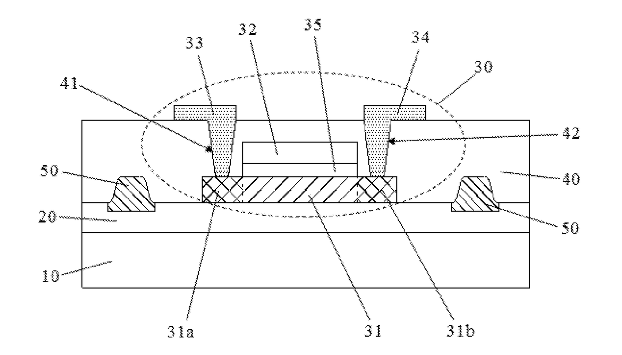
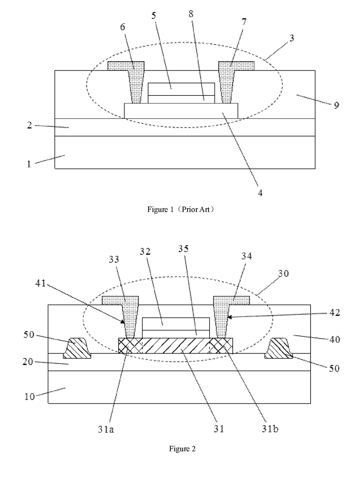
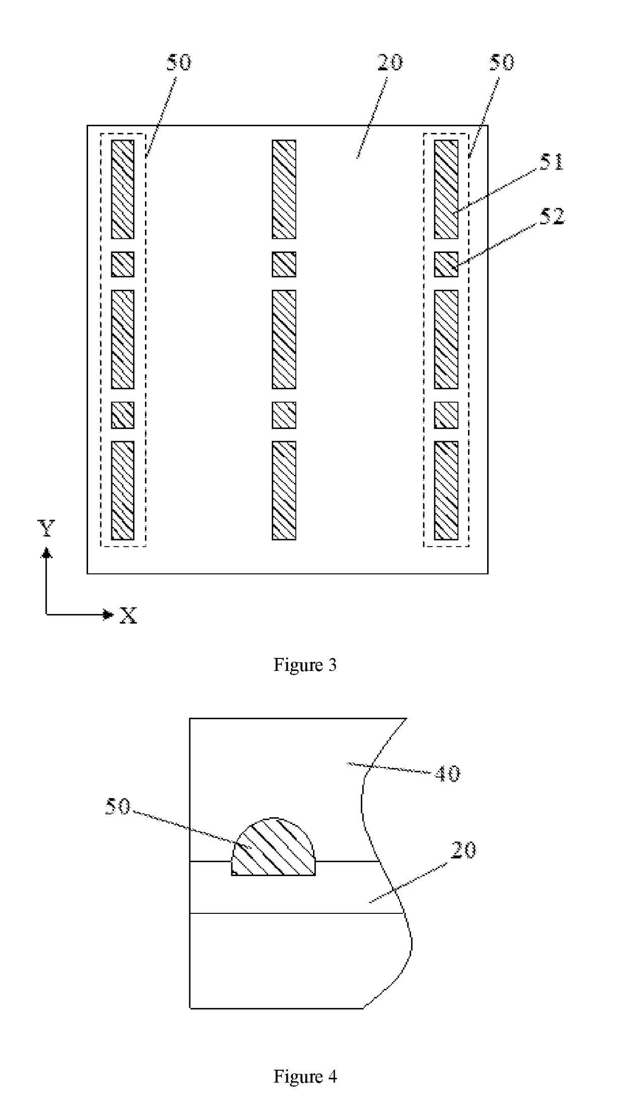
[0025]First, the present embodiment provides a flexible array substrate, as shown in FIG. 2. The flexible array substrate comprises a flexible substrate 10 and a buffer layer 20 on the flexible substrate 10. Multiple thin f...


PUM


Abstract

The present disclosure discloses a flexible array substrate, comprising a flexible substrate and a buffer layer on the flexible substrate. Multiple thin film transistors are provided on the buffer layer in array. An interlayer dielectric layer is provided on the thin film transistor. The interlayer dielectric layer covers the buffer layer. Wherein, an interconnecting structure is provided between the interlayer dielectric layer and the buffer layer. At least one interconnecting structure is respectively provided at both sides of each column of the thin film transistor. The interconnecting structure extends toward the direction parallel to the bending axis of the flexible array substrate. The present disclosure further discloses a preparation method of flexible array substrate and a flexible display device with the flexible array substrate. The present disclosure provides the interconnecting structure, which enhances the connecting performance of the interconnecting layer in the flexible array substrate.

Description

BACKGROUND OF THE INVENTION1. Field of the Invention[0001]The present disclosure relates to the fields of display technology, and in particular to a flexible array substrate and the preparation method thereof, and further to a flexible display device with above flexible array substrate.2. The Related Arts[0002]In recent years, flat panel display technology has been rapid developed, no matter the size of the screen or the display quality have made great progress. With its bending properties, the flexible display device can be competent in many areas requiring surface display, such as various fields of smart cards, electronic paper, smart labels, as well as the conventional flat panel display device which can be applied to. The flexible display device will occupy a huge market in the future display market with its dreamy and beautiful appearance. Typically, the flexible display device includes stacked flexible array substrates and electroluminescent devices. A transparent flexible cov...

Claims


Application Information

Patent Timeline
IPC IPC(8): H01L51/00H01L51/05H01L51/50H01L51/52H01L51/56
CPCH01L51/0097H01L51/0516H01L51/5056H01L51/5072H01L51/5206H01L51/5221H01L51/56H01L27/1218H01L27/1259H10K59/12Y02E10/549H01L29/78603H01L27/1244Y02P70/50H10K59/124H10K59/131H10K77/111H10K2102/311H10K10/468H10K50/15H10K50/16H10K50/81H10K50/82H10K71/00
Inventor QIN, FANG
Owner WUHAN CHINA STAR OPTOELECTRONICS TECH CO LTD
Why Eureka
Try Eureka