Method and system for integrated differential electro-absorption modulator device

a technology of differential electroabsorption and modulator, applied in non-linear optics, instruments, optics, etc., can solve the problems of large bandwidth, limited popular applications, and large amount of data transferred, and achieve the effect of optimizing the advantages of configuration

Active Publication Date: 2018-11-08
MARVELL ASIA PTE LTD
View PDF16 Cites 3 Cited by
  • Summary
  • Abstract
  • Description
  • Claims
  • Application Information

AI Technical Summary

Benefits of technology

[0008]The differential nature of the driver allows the ability to produce larger drive voltages, which provide balance for better signal integrity at the driver, transmission lines, and on the diode load. The termination resistor can be configured to reduce signal reflections without affecting the configuration of the first and second EAM modules. In a specific embodiment, the first impedance can be predetermined as a data line impedance, which can be the same as the second impedance. In various embodiments, the impedances of these transmission lines can be configured as symmetrical or asymmetrical depending on the application.
[0010]Many benefits are recognized through various embodiments of the present invention. Such benefits include having a beneficial configuration for RF layouts. Embodiments of this configuration also allows a faster driver transistor with lower breakdown voltage to directly apply the data signals, while the necessary DC bias can be generated by a slower, higher breakdown voltage transistor. Embodiments of the driver circuit can be fully integrated in a nanoscale CMOS process using fast low-V and slow high-V devices to maximize these advantages. The driver can also be directly coupled to modulators on a photonic IC without the need for external passive components other than patterned metal lines. Other benefits will be recognized by those of ordinary skill in the art that the mechanisms described can be applied to other communications systems as well.

Problems solved by technology

In the early days of the Internet, popular applications were limited to emails, bulletin board, and mostly informational and text-based web page surfing, and the amount of data transferred was relatively small.
Today, Internet and mobile applications demand a huge amount of bandwidth for transferring photo, video, music, and other multimedia files.
These limitations provide significant challenges to the continued improvement of communication systems scaling and performance.
Unfortunately, they have been inadequate for various applications.

Method used


Image

  • Method and system for integrated differential electro-absorption modulator device
  • Method and system for integrated differential electro-absorption modulator device
  • Method and system for integrated differential electro-absorption modulator device

Examples


Embodiment Construction

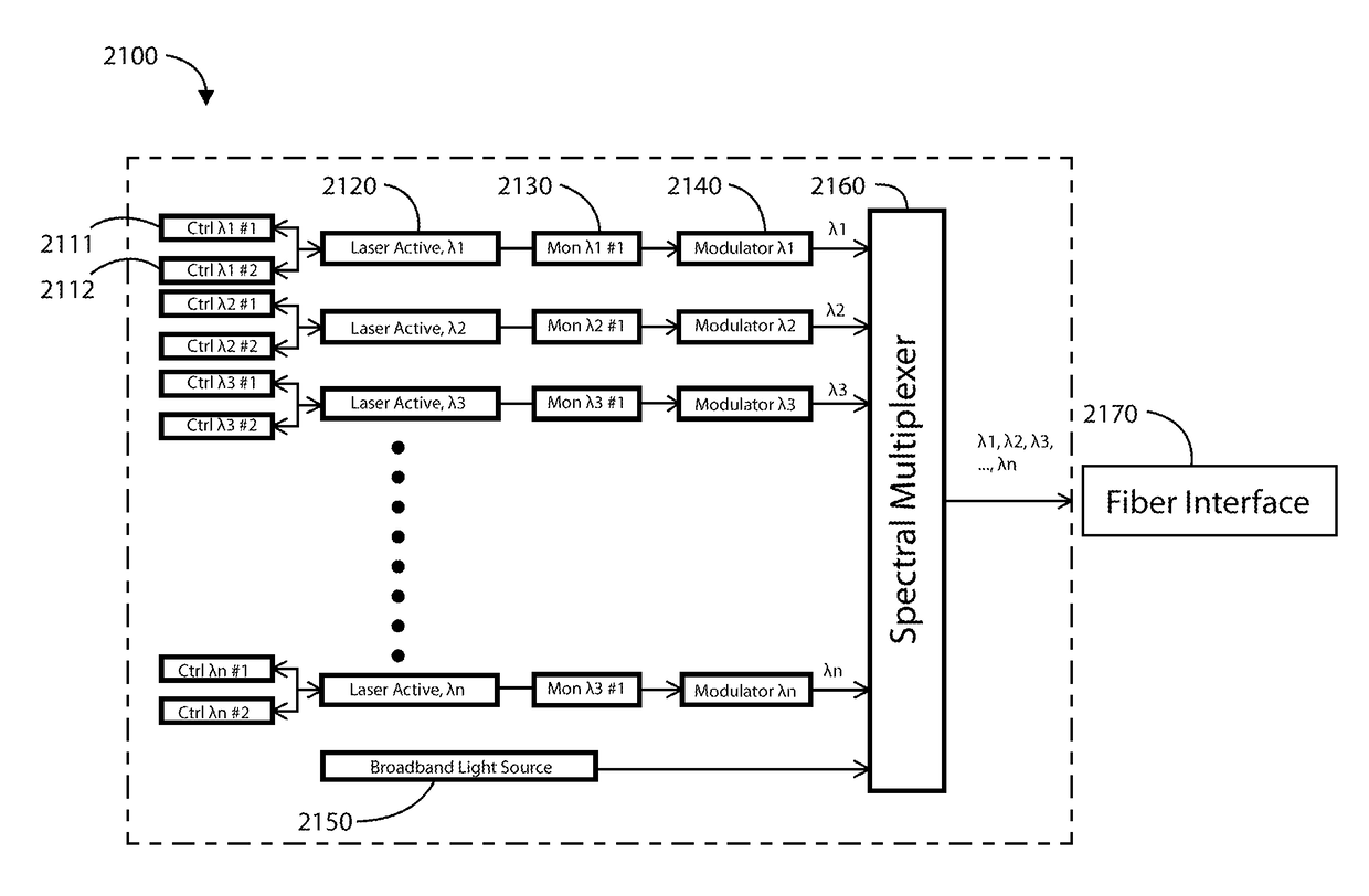
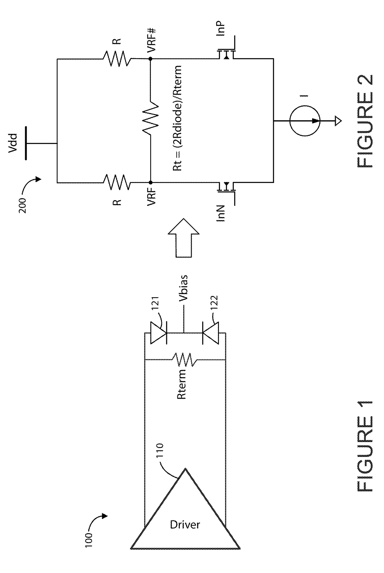
[0039]The present invention relates to telecommunication techniques and integrated circuit (IC) devices. More specifically, various embodiments of the present invention provide an integrated differential Electro-Absorption Modulator (EAM) device. The modulator device can include an electrical driver circuit configured overlying a substrate member and coupled to a first and second EAM module. These EAM modules can be coupled to a common mode termination resistor, a beam splitter module, and a bias circuit. Furthermore, the differential EAM device can be coupled within a communication interface configured to transfer data at high bandwidth over optical communication networks.

[0040]The following description is presented to enable one of ordinary skill in the art to make and use the invention and to incorporate it in the context of particular applications. Various modifications, as well as a variety of uses in different applications will be readily apparent to those skilled in the art, ...


PUM

PropertyMeasurementUnit
bias voltageaaaaaaaaaa
breakdown voltageaaaaaaaaaa
voltageaaaaaaaaaa

Abstract

An integrated differential Electro-Absorption Modulator (EAM) device. The device includes a substrate, an electrical driver, and two EAM modules. The electrical driver circuit is configured overlying the substrate member and has one output electrically coupled to the first EAM module and the other output electrically coupled to the second EAM module. The first and second EAM modules have a first and a second output, respectively. A beam splitter can be configured to split an optical input into two optical outputs, each of which can be optically coupled to the optical inputs of the first and second EAM modules.

Description

CROSS-REFERENCE TO RELATED APPLICATIONS[0001]This application is a continuation of U.S. patent application Ser. No. 14 / 226,713 filed Mar. 26, 2014, which is incorporated by reference herein.BACKGROUND OF THE INVENTION[0002]The present invention relates to telecommunication techniques and integrated circuit (IC) devices. More specifically, various embodiments of the present invention provide an integrated differential Electro-Absorption Modulator (EAM) device. The modulator device can include an electrical driver circuit configured overlying a substrate member and coupled to a first and second EAM module. These EAM modules can be coupled to a common mode termination resistor, a beam splitter module, and a bias circuit. Furthermore, the differential EAM device can be coupled within a communication interface configured to transfer data at high bandwidth over optical communication networks.[0003]Over the last few decades, the use of communication networks has exploded. In the early days...

Claims


Application Information

Patent Timeline
Patent Type & Authority Applications(United States)
IPC IPC(8): G02F1/025
CPCG02F1/025G02F1/0121G02F1/0123G02F1/2257G02F2201/58G02F1/0155
Inventor NAGARAJAN, RADHAKRISHNAN L.
Owner MARVELL ASIA PTE LTD
Why Eureka
Try Eureka