Blue phase liquid crystal modules, blue phase liquid crystal devices, and the manufacturing method thereof
a liquid crystal module and blue phase technology, applied in non-linear optics, instruments, optics, etc., can solve the problems of large driving voltage, low development cost, and inability to obtain the light state of the liquid crystal panel, so as to reduce the driving voltage of the blue phase liquid crystal module
- Summary
- Abstract
- Description
- Claims
- Application Information
AI Technical Summary
Benefits of technology
Problems solved by technology
Method used
Image
Examples
third embodiment
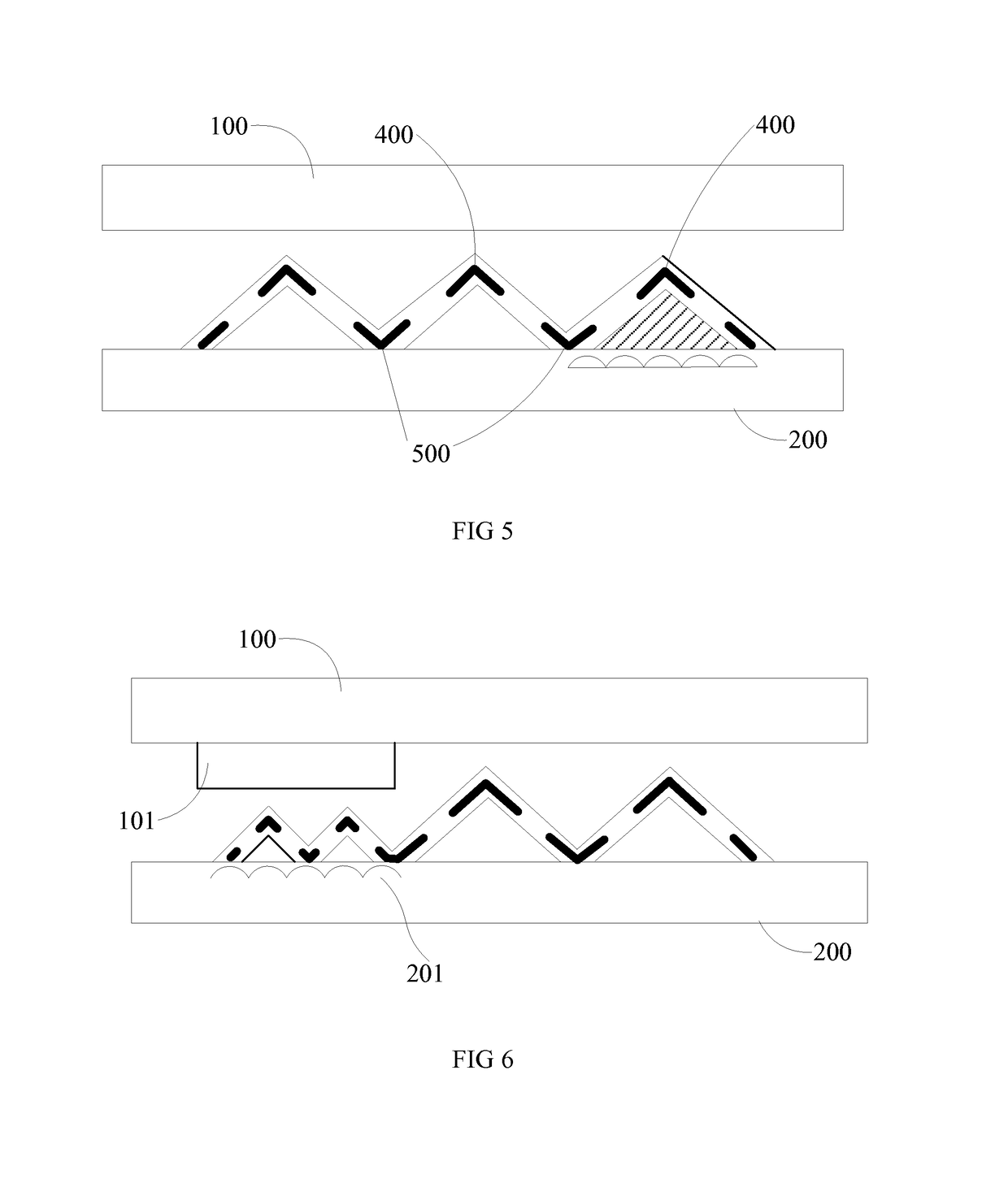
[0056]FIG. 6 is a cross-sectional view of the blue phase liquid crystal module in accordance with a In the embodiment, the height of the insulation layer 700 in the transmission area is larger than the height of the insulation layer 700 in the reflective area such that the thicknesses of the blue phase liquid crystals in the transmission area and in the reflective area are different. In this way, the transmission area may own a larger phase delay, and the transmission area and the reflective area may have consistent optical characteristics.
[0057]It is to be noted that the gap between the electrodes may be the same or may be similar. At the same time, in order to save the blue phase liquid crystals, a flat layer 101 may be configured on the peak of the insulation layer 700 having the smaller height. The flat layer 101 may operates as stuffing, and is made by transparent materials.
[0058]In the third embodiment, the height of the insulation layer 700 in the transmission area is larger...
fourth embodiment
[0059]FIG. 7 is a cross-sectional view of the blue phase liquid crystal module in accordance with a The transmission area and the reflective area are spaced apart from the up substrate 100 respectively for the gap D1 and D3, wherein D1 and D3 are larger than the gap D2 between the auxiliary mats and the up substrate or the down substrate. In this way, when the blue phase liquid crystal module is pressed, as the auxiliary mats abuts against the up substrate or the down substrate, the protrusive common electrode or the pixel electrode are protected.
fifth embodiment
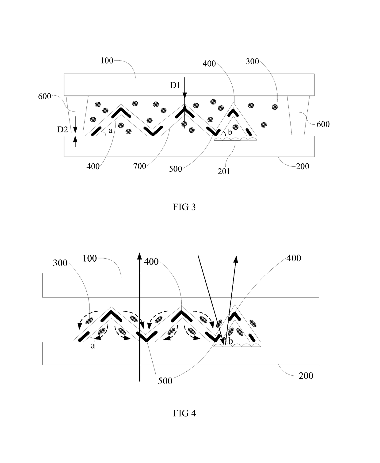
[0060]In the fifth embodiment, the insulation layer 700 may be of one-layer structure. FIG. 8 is a schematic view of the blue phase liquid crystal module of FIG. 3, wherein only one insulation layer is provided. In the embodiment, the insulation layer 700 is only provided below the pixel electrode 500 and the common electrode 400 to support the pixel electrode 500 and the common electrode 400.
[0061]In the above disclosure relating to the second embodiment to the fifth embodiment, the details the same with that in the first embodiment are omitted hereinafter.
[0062]Compared to the conventional technology, the blue phase liquid crystal module is configured with the hollow or solid insulation layer having the down substrate as the bottom. In addition, the V-shaped or inverse-V-shaped pixel electrode and common electrode may be embedded within the insulation layer. The blue phase liquid crystals are driven by the slant electrical field formed between the V-shaped and the inverse-V-shaped...
PUM
| Property | Measurement | Unit |
|---|---|---|
| included angle | aaaaa | aaaaa |
| included angle | aaaaa | aaaaa |
| included angle | aaaaa | aaaaa |
Abstract
Description
Claims
Application Information


