Eureka AIR delivers breakthrough ideas for toughest innovation challenges, trusted by R&D personnel around the world.

Optical modulation method for a liquid crystal layer and liquid crystal device using the method

a liquid crystal layer and optical modulation technology, applied in the optical field, can solve the problems of a great deal of time and effort to find a new liquid crystal material, and its reliability is in doubt, and achieve the effect of excellent performance in practical us

Inactive Publication Date: 2009-12-01
INNOLUX CORP
View PDF7 Cites 0 Cited by
  • Summary
  • Abstract
  • Description
  • Claims
  • Application Information

AI Technical Summary

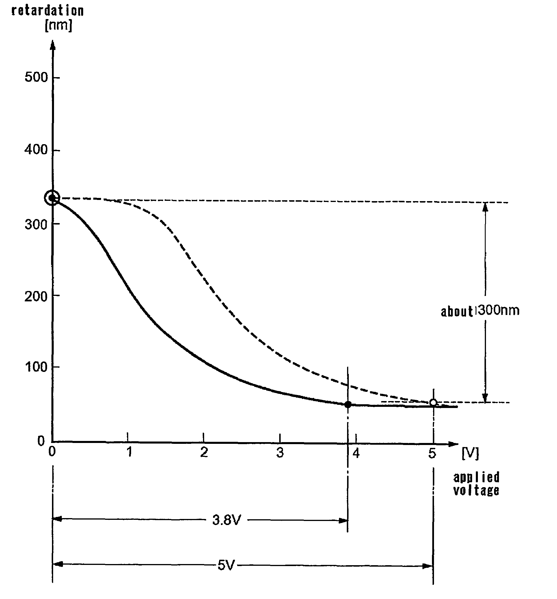
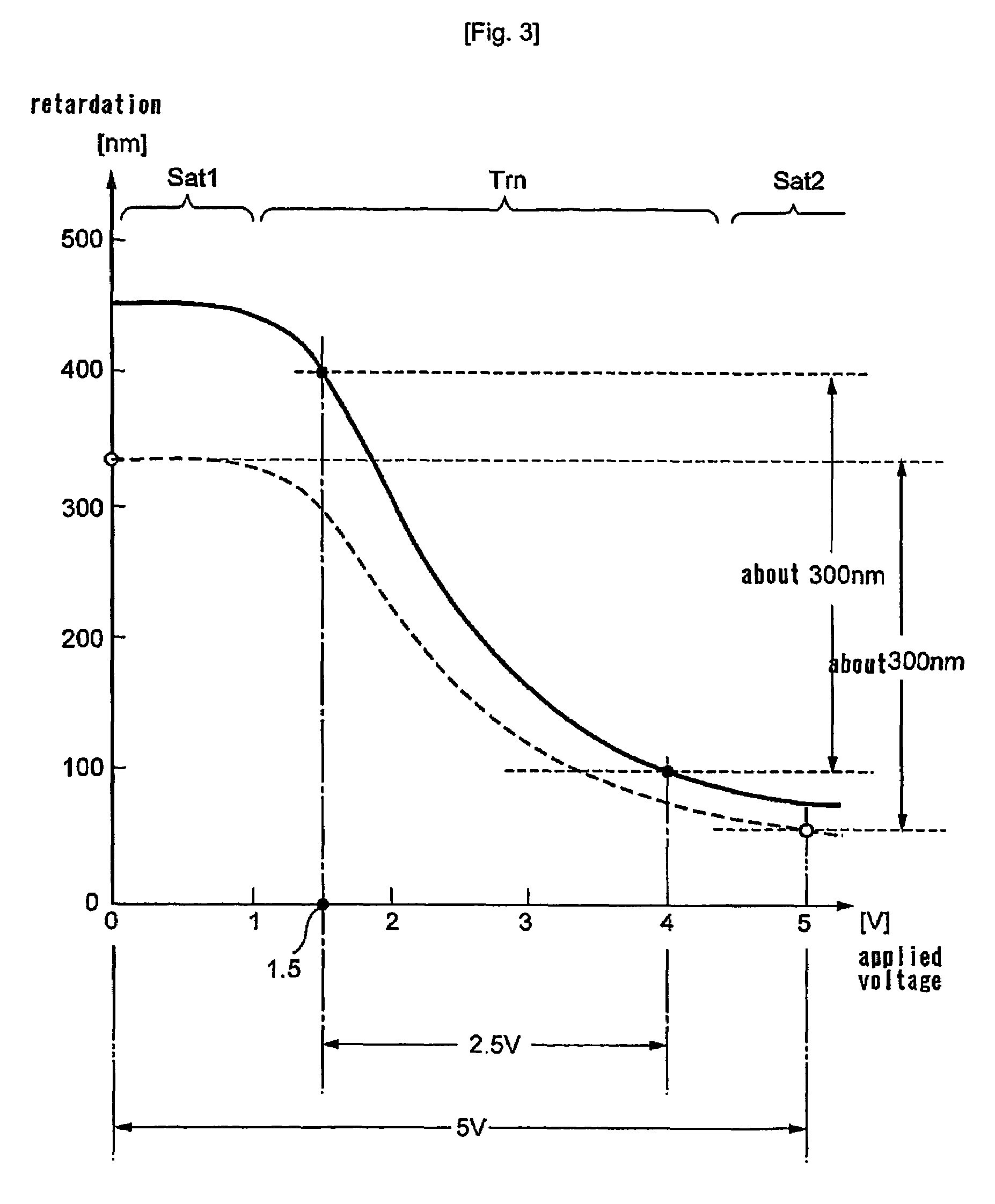
Benefits of technology

[0008]The present invention has been made in view of the foregoing, its object is to provide an optical modulation method for a liquid crystal layer and a liquid crystal device using the method, which can satisfactorily present a bright state and a dark state with a low driving voltage without changing a liquid crystal material.
[0009]Another object of the invention is to provide an optical modulation method for a liquid crystal layer and a liquid crystal device using the method, which can reliably present a bright state and a dark state without changing a liquid crystal material while contributing to reduction of power consumption.
[0010]A further object of the invention is to provide reflective type, transmissive type and transflective type liquid crystal devices which can contribute to reduction of power consumption without changing a liquid crystal material.
[0012]In this way, it is possible to decrease the maximum driving voltage of the liquid crystal layer and to narrow a driving voltage range, and thereby contribute to power saving. In addition, since this method is not dependent on characteristics of the liquid crystal material in itself, it is possible to provide a power saving technique having its broad scope of application. More specifically, the difference is substantially 5 V between the predetermined high voltage and the predetermined low voltage, and the liquid crystal layer conventionally driven in a range of 5 V can be driven with a voltage less than 5 V without changing the capability of presenting a bright state and a dark state.
[0014]It is thereby possible to suppress the driving energy of the liquid crystal layer and thus contribute to reduction of power consumption in the entire device.
[0017]In each aspect described above, the device may have phase compensation means between the front polarizing plate and the liquid crystal layer, and / or between the liquid crystal layer and the rear polarizing plate. It is thus possible to obtain extremely excellent performance in practical use.

Problems solved by technology

However, the method, first of all, requires a great deal of time and efforts to find a new liquid crystal material capable of being driven with a desired low voltage.
Further, even if such a new material was found, there would be cases where its reliability is in doubt in other technical aspects, for example, about whether the durability, operation stability and more are adequate.

Method used


Image

  • Optical modulation method for a liquid crystal layer and liquid crystal device using the method
  • Optical modulation method for a liquid crystal layer and liquid crystal device using the method
  • Optical modulation method for a liquid crystal layer and liquid crystal device using the method

Examples


first embodiment

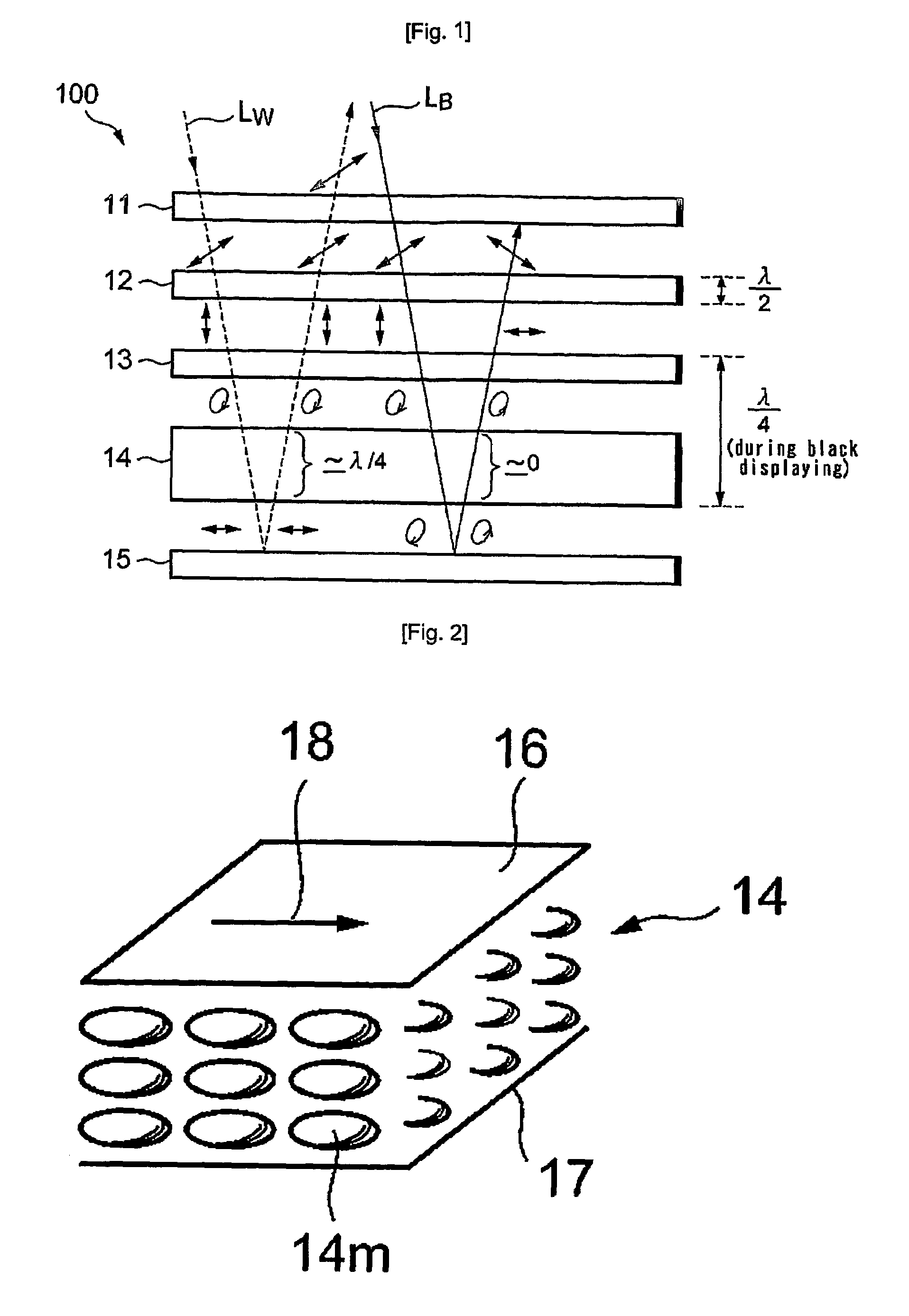
[0030]FIG. 1 schematically shows a sectional construction of a liquid crystal display device according to one embodiment of the invention.

[0031]A liquid crystal display device 100 is a reflective type liquid crystal display device, and has an arrangement of a linearly polarizing plate 11, a first retardation film 12 that is a half-wave plate, a second retardation film 13 that is a quarter-wave plate, a liquid crystal layer 14 which is sandwiched by a pair of electrodes (not shown) that apply a voltage corresponding to pixel information to be displayed, and an optical reflective layer 15, in this order from the front side that is the display screen side. The linearly polarizing plate 11, and the first and second retardation films 12, 13 forms means having a function of the right-hand or left-hand circular polarization. It is noted that only principal structure elements are described herein for the sake of clarity of description, but other structural elements may be actually included ...

second embodiment

[0053]FIG. 6 schematically shows a cross sectional construction of a liquid crystal display device according to another embodiment of the invention.

[0054]A liquid crystal display device 200 is a transmissive type liquid crystal display device, and has: the linearly polarizing plate 11; the first retardation film 12 that is a half-wave plate; the second retardation film 13 that is a quarter-wave plate; the liquid crystal layer 14 which is sandwiched by a pair of electrodes (not shown) that apply a voltage corresponding to pixel information to be displayed to the layer 14; a third retardation film 21 that is a quarter-wave plate; a fourth retardation film 22 that is a half- wave plate; and a rear linearly polarizing plate 23. The linearly polarizing plate 11, the first and second retardation films 12, 13 form means having one of the right-hand and left-hand circularly polarizing functions, and the third and fourth retardation films 21, 22 and the rear linearly polarizing plate 23 form...

third embodiment

[0063]FIG. 7 schematically shows a cross sectional construction of a liquid crystal display device according to a further embodiment of the invention.

[0064]A liquid crystal display device 300 is a transflective type liquid crystal display device, and basically has the construction having an optical reflective layer 31 arranged between the liquid crystal layer 14 and the third retardation film 21 in addition to the construction of the transmissive type liquid crystal display device 200 as described above. The optical reflective layer 31 basically forms a reflective area within each pixel, and the other area is formed as a transmissive area The optical reflective layer 31 may be formed to also serve as a pixel electrode.

[0065]The other structural aspect and behavior of incident light can be described in the same way as in the reflective type liquid crystal display device 100 and transmissive type liquid crystal display device 200 respectively described in the First and Second Embodime...


PUM

PropertyMeasurementUnit
voltageaaaaaaaaaa
thicknessaaaaaaaaaa
pre-tilt angleaaaaaaaaaa

Abstract

An object of the invention is to satisfactorily present a bright state and a dark state with a low driving voltage without changing a liquid crystal material. A liquid crystal device 100 having a configuration wherein a polarizing plate 11, a liquid crystal layer 14 and an optical reflective layer 15 are arranged in this order from the front side of the device. The liquid crystal layer 14 is capable of providing one retardation when the liquid crystal layer is applied with a predetermined high voltage and providing the other retardation when the liquid crystal layer is applied with a predetermined low voltage, for light that is incident from the polarizing plate 11, passes through the liquid crystal layer, reflects on the optical reflective layer 15, passes again through the liquid crystal layer 14 and is guided to the polarizing plate 11, whereby a bright state and a dark state are presented based on a difference between these retardations. A thickness of the liquid crystal layer and / or a pre-tilt angle of liquid crystal molecules of the liquid crystal layer is made to be greater than in the case where the one and the other retardations are provided, so that a difference between a first retardation obtained by applying the liquid crystal layer with a modified high voltage lower than the predetermined high voltage and a second retardation obtained by applying the liquid crystal layer with a modified low voltage equal to or higher than the predetermined low voltage, for example is made to be substantially half of wavelength of the light.

Description

BACKGROUND OF THE INVENTION[0001]1. Field of the Invention[0002]The present invention generally relates to an optical modulation method for a liquid crystal layer. The invention relates to a liquid crystal device or liquid crystal display device using such an optical modulation method. The invention also relates to a driving method for a liquid crystal layer whose liquid crystal molecules forming the upper and bottom surfaces of the layer have their alignment directions parallel to each other for the upper and the bottom, and to a liquid crystal device or liquid crystal display device based on the driving method.[0003]2. Description of the Related Art[0004]Conventionally, there have been proposed various methods for reducing power consumption in a liquid crystal display device. The liquid crystal display device is comprised of a variety of structural elements, and in terms of each of the structural elements, many kinds of methods are considered for reducing power consumption. For ex...

Claims


Application Information

Patent Timeline
Patent Type & Authority Patents(United States)
IPC IPC(8): G02F1/133G02F1/1335G02F1/13363G02F1/139
CPCG02F1/1393G02F1/13306G02F2203/02G02F2202/40G02F2001/133638G02F1/133638G02F1/1335G02F1/136
Inventor SHIBAZAKI, MINORU
Owner INNOLUX CORP
Why Eureka
Eureka Blog
Learn More