Organic electroluminescent device and method of manufacture thereof

a technology of electroluminescent devices and organic light-emitting layers, which is applied in the direction of discharge tube luminescnet screens, natural mineral layered products, transportation and packaging, etc., can solve the problems of increased driving voltage, easy deterioration of organic light-emitting layers, and easy leakage curren

Inactive Publication Date: 2002-07-09
IDEMITSU KOSAN CO LTD
View PDF11 Cites 166 Cited by
  • Summary
  • Abstract
  • Description
  • Claims
  • Application Information

AI Technical Summary

Problems solved by technology

However, because the organic light-emitting layer is an organic substance, injecting electrons from a cathode layer is not easy.
In addition, because the organic substance generally can transfer electrons and positive holes only with difficulty, the organic light-emitting layer tends to deteriorate easily and produce leakage current when used for a long period of time.
However, the inorganic compounds such as aluminum nitride, tantalum nitride, SiO.sub.2, and the like used as an insulating thin layer in the organic EL devices disclosed in Japanese Patent Application Laid-open No. 8-288069 and U.S. Pat. No. 5,853,905 have a great ionization potential which results in an increased driving voltage.
Specifically, because the inorganic thin layers consisting of these inorganic compounds are electric insulating layers having an excessively large ionization energy, positive holes are injected from the anode layer by a tunnel effect.
The organic EL device disclosed in Japanese Patent Application Laid-open No. 9-260063 is characterized by the use of NiO as a major component, which unduly limits the types of materials usable as an inorganic material layer and exhibits only a low luminous efficiency.
The organic EL device disclosed in Japanese Patent No. 282411 has the problems of small positive hole mobility and insufficient durability in spite of the use of the metal oxide materials such as RuO.sub.x (1.ltoreq.x.ltoreq.2), MoO.sub.3, and V.sub.2 O.sub.5.
Therefore, the light transmittance in the visible radiation range of the anode layer made of these metal oxide materials is very low, for example, about 1/9 to 1/5 that of ITO, giving rise to problems such as a poor luminous efficiency and a small quantity of light which can be emitted.
Such an anode layer cannot be used in practice.
Moreover, when an anode layer having such a two-layer structure is fabricated, the thickness of the ITO and a metal oxide film must be restricted within a prescribed range, resulting in a limitation in the manufacturing process.
This is because high resistance of the electrode layer prevents uniformity of luminescence.
If either the group A or the group B is solely used, it is difficult to form an intermediate level in the inorganic thin layer.
Therefore, it is impossible to decrease the driving voltage or improve d

Method used


Image

  • Organic electroluminescent device and method of manufacture thereof
  • Organic electroluminescent device and method of manufacture thereof
  • Organic electroluminescent device and method of manufacture thereof

Examples


example 1

(1) Preparation for Manufacturing Organic EL Device

Before manufacturing the organic EL device of Example 1, a transparent electrode layer with a thickness of 75 nm was formed from ITO as an anode layer on a transparent glass substrate with a dimension of thickness:1.1 mm.times.length:25 mm.times.width:75 mm. The glass substrate and the anode layer are collectively called a substrate in the following description. This substrate was ultrasonically washed in isopropyl alcohol, dried in a nitrogen gas atmosphere, and washed for 10 minutes using UV (ultraviolet radiation) and ozone.

(2) Formation of Inorganic Thin Layer

Next, the substrate on which an anode layer has been formed was placed in a vacuum vessel for common use as a radio frequency sputtering apparatus and a vacuum deposition apparatus. A target consisting of tin oxide and ruthenium oxide (at a ratio of 10:1) to form an inorganic thin layer was installed in the vacuum vessel. After reducing the pressure in the vacuum vessel to ...

fifth embodiment

The method of the followed in simultaneously depositing vaporized DPVTP and DPAVBi. Specifically, in forming the organic light-emitting layer, the vapor deposition material containers 212B and 212C were respectively arranged at positions at a distance from the rotation axis line of the substrate of 30 mm in the horizontal direction, and the containers were heated in this positional arrangement to simultaneously vaporize DPVTP and DPAVBi, while rotating the substrate around the rotation axis at 5 rpm.

Next, Alq was vaporized from the vapor deposition material containers 212D under the following conditions to form an An electron injection layer on the organic light-emitting layer.

Alq vaporization rate: 0.2 nm / s

Alq thickness: 5 nm

Finally, Al and Li were vaporized respectively from the vapor deposition material containers 212E and 212F to form a cathode layer on the electron injection layer, thereby providing an organic EL device.

Al vaporization rate: 1 nm / s

Li vaporization rate: 0.01 nm / ...

examples 2 to 4

In Examples 2 to 4, organic EL devices were prepared in the same manner as in Example 1, except for changing the types of inorganic compounds and the amounts of the components as shown in Table 3. Luminous brightness and the like were evaluated.

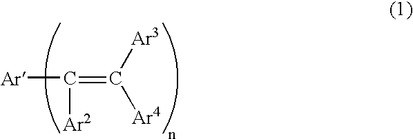
As shown in Table 3, the ionization potential of the inorganic thin layer of each Example was 5.4 eV or more. This is presumed to be due to an intermediate level formed in the inorganic thin layer. The ionization energy of DPVTP which is an organic light-emitting material was 5.9 eV, confirming that the value is greater than the intermediate level (an energy value) of the inorganic thin layer.


PUM

PropertyMeasurementUnit
Thicknessaaaaaaaaaa
Percent by atomaaaaaaaaaa

Abstract

An organic EL device having a low driving voltage and exhibiting high luminous brightness and superior durability, and a method of manufacturing the same. The organic EL device has an anode layer, an organic light-emitting layer, and a cathode layer. An inorganic thin layer, comprising an inorganic compound of Ge, Sn, Zn, Cd, etc. and an inorganic compound of an element of Group 5A to Group 8 in the periodic table in combination, is provided between the anode layer and the organic light-emitting layer and between the cathode layer and the organic light-emitting layer, or the anode layer or the cathode layer comprises a chalcogenide of Si, Ge, Sn, Pb, Ga, In, Zn, Cd, Mg, etc. and an inorganic compound of an element of Group 5A to Group 8 in the periodic table in combination.

Description

The present invention relates to an organic electroluminescent device (hereinafter may be called "organic EL device") and a method of manufacturing the organic EL device. More particularly, the present invention relates to an organic EL device suitably used for display apparatuses for home use or industrial use, light sources for printer heads, and the like, and to a method of manufacturing the organic EL devices.DESCRIPTION OF THE BACKGROUNDDevelopment of organic EL devices with an organic light-emitting layer inserted between electrodes of the devices have intensively been undertaken for the following reasons.(1) Handling and production of organic EL devices become easy because the organic EL devices are complete solid elements.(2) Organic EL devices do not require the additional luminous apparatuses because these devices can emit the light themselves.(3) Organic EL devices are suitable for use with display apparatuses due to excellent visibility.(4) A full color display can be ea...

Claims


Application Information

Patent Timeline
IPC IPC(8): H01L51/52H01L51/50
CPCH01L51/5088H01L51/5092H01L51/5221H01L51/5206H01L51/5012Y10T428/26Y10T428/24942H10K50/11H10K50/17H10K50/171H10K50/81H10K50/82H05B33/22
Inventor KAWAMURA, HISAYUKINAKAMURA, HIROAKIHOSOKAWA, CHISHIO
Owner IDEMITSU KOSAN CO LTD
Why Eureka
Try Eureka