Display device and method for manufacturing thereof

a technology of a display device and a manufacturing method, applied in the direction of discharge tube luminescnet display, discharge tube/lamp details, electric discharge lamps, etc., can solve problems such as drive voltage, achieve excellent reliability and heat resistance, and reduce short circuit defects , the effect of low drive voltag

Inactive Publication Date: 2007-04-03
SEMICON ENERGY LAB CO LTD
View PDF20 Cites 180 Cited by
  • Summary
  • Abstract
  • Description
  • Claims
  • Application Information

AI Technical Summary

Benefits of technology

[0021]Therefore, it is an object of the present invention to apply a conductive buffer layer using a polymer to a display device formed by arranging organic light-emitting elements as pixels in a matrix form without causing crosstalk. Also, it is a problem to provide, by the above, a display device which is low in drive voltage, excellent in reliability and heat resistance, and less in defects of short circuits or the like.

Problems solved by technology

Also, it is a problem to provide, by the above, a display device which is low in drive voltage, excellent in reliability and heat resistance, and less in defects of short circuits or the like.
Furthermore, it is a problem to provide an electric apparatus less in consumption power and long in life by the manufacture using the display device.

Method used


Image

  • Display device and method for manufacturing thereof
  • Display device and method for manufacturing thereof
  • Display device and method for manufacturing thereof

Examples


embodiment 1

[Embodiment 1]

[0083]This embodiment exemplifies a passive matrix display device by taking the display device for instance that is disclosed in the present invention. FIG. 5A shows a top view thereof and FIG. 5B shows a sectional view taken along the line P–P′ of FIG. 5A.

[0084]In FIG. 5A, reference numeral 501 denotes substrate, a plastic material and glass are used for forming the substrate. As the plastic material, polyimides, polyamides, acrylic resins, epoxy resins, PESs (polyethersulfones), PCs (polycarbonates), PETs (polyethylene terephthalates), or PENs (polyethernitriles) can be used in state of a sheet or a film.

[0085]Reference numeral 502 denotes scanning lines (anodes) formed from a conductive oxide film. The conductive oxide film used in this embodiment is obtained by indium tin oxide (ITO) that is transparent to the visible light. Denoted by reference numeral 506 are data lines (cathodes) comprising of a metal film. The data lines are formed of stripe patterns by using C...

embodiment 2

[Embodiment 2]

[0090]In this embodiment an explanation will be given of a display device comprising the organic light-emitting device disclosed in the present invention. FIG. 6 is a diagram illustrating an active matrix type display device. The FIG. 6A illustrates a view of top surface. FIG. 6B illustrates a cross sectional view of FIG. 6A taken along the line P–P′.

[0091]Note that although thin film transistors (referred to as TFTs hereinafter) are used as active devices in this embodiment, MOS transistors may also be used. Additionally, although top gate type TFTs (practically planar type TFTs) will be exemplified as the TFTs, bottom gate type TFTs (typically, inversely staggered TFTs) is alternatively used.

[0092]With reference to FIGS. 6A–B, reference numeral 601 denotes a substrate. In order to observe the light through the substrate in the display device, the substrate must be transparent to the visible light. Practically, a glass substrate, a quartz substrate, a crystallized gla...

embodiment 3

[Embodiment 3]

[0105]This embodiment exemplifies an active matrix display device by taking the display device for instance. In this embodiment the display device having a configuration in which light is emitted through the opposite substrate attached active devices (hereinafter referred to as top emission) is demonstrated, which is different from the configuration illustrated in Embodiment 2. FIG. 7 shows a sectional view thereof.

[0106]Note that although thin film transistors (referred to as TFTs hereinafter) are used as active devices in this embodiment, MOS transistors may also be used. Additionally, although top gate type TFTs (practically planar type TFTs) will be exemplified as the TFTs, bottom gate type TFTs (typically, inversely staggered TFTs) is alternatively used.

[0107]In this embodiment, except a first electrode, a second electrode, a protection film, and cover member may have the same structures as those illustrated in Embodiment 2.

[0108]Since the first electrode 602 conn...


PUM


Abstract

It is a problem to provide an electric apparatus less in consumption power and long in life by the manufacture using the display device.
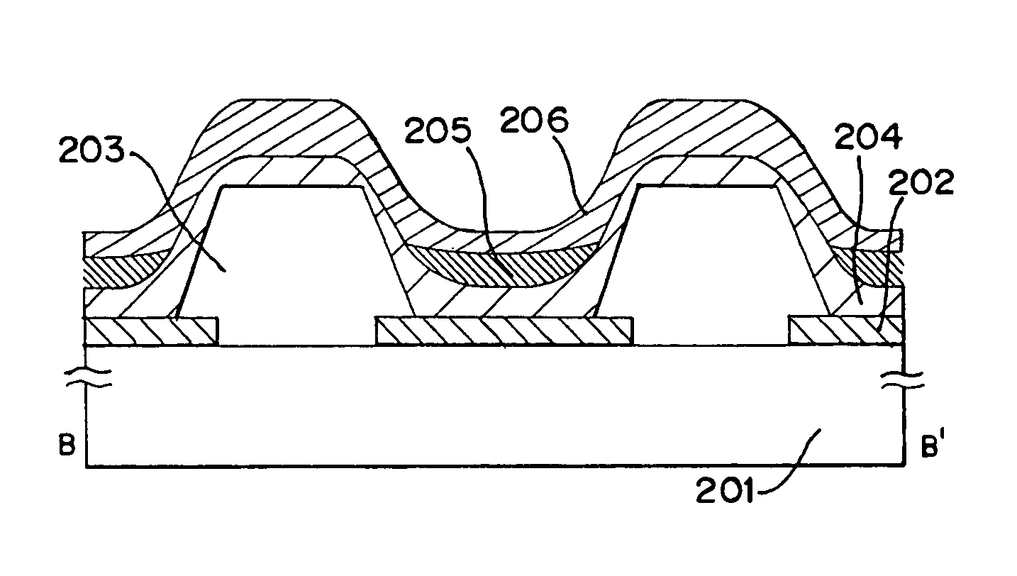
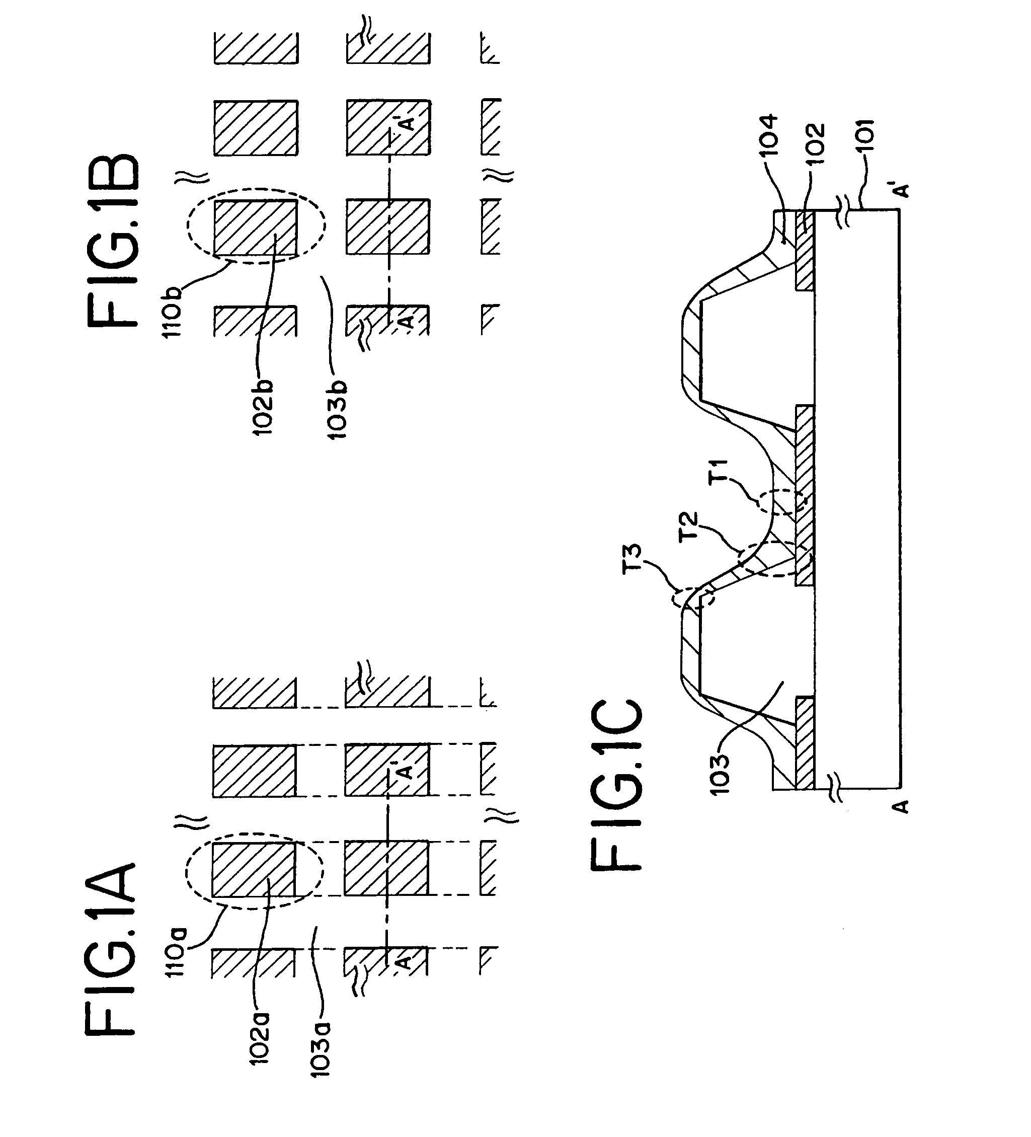
An insulating bank 103a is provided in a form surrounding the pixel portions 110a on first electrodes 102a over a substrate. The entire surface is applied, by a wet scheme(method), with an organic conductive film 104. The organic conductive film 104 has a thickness form of T2>T1>T3 under the influence of the insulating bank 103. Accordingly, the portion T3 has an increased resistance in a lateral direction, making possible to prevent against crosstalk. Due to a conductive polymer as a buffer layer 104, a display device can be provided which is low in drive voltage. Furthermore, because the portion T2 is increased in thickness, the electric-field concentration is relaxed at and around the pixel portion. This makes it possible to prevent the organic light-emitting element from deteriorating at around the pixel.

Description

BACKGROUND OF THE INVENTION[0001]1. Field of the Invention[0002]The present invention relates to a display device using an organic light-emitting device that has an anode, a cathode, and a film containing an organic compound that emits light by application of electric field (hereinafter referred to as organic thin film). Specifically, the present invention relates to a high reliable display device that drives at a low voltage. The organic thin film contains an organic compound as light-emitting compounds, and also may contain an inorganic compound as another component elements. The term display device in this specification refers to an image display device that employs the organic light-emitting device as a light-emitting device. Also included in the definition of the display device are: a module in which a connector, such as an anisotropic conductive film (FPC: flexible printed circuit), a TAB (tape automated bonding) tape, or a TCP (tape carrier package), is attached to the organi...

Claims


Application Information

Patent Timeline
Patent Type & Authority Patents(United States)
IPC IPC(8): H01L51/00H01L27/32H01L51/50
CPCH01L27/3246H01L51/5203H05B33/10H01L27/32H01L51/5088H01L27/3283H01L51/5052H10K59/122H10K59/173H10K50/155H10K50/165H10K50/17H10K50/805H10K59/00
Inventor SEO, SATOSHIYAMAZAKI, SHUNPEI
Owner SEMICON ENERGY LAB CO LTD
Why Eureka
Try Eureka