

Electroluminescent host material
- Summary
- Abstract
- Description
- Claims
- Application Information
AI Technical Summary
Benefits of technology
Problems solved by technology
Method used
Image

Examples
embodiment a
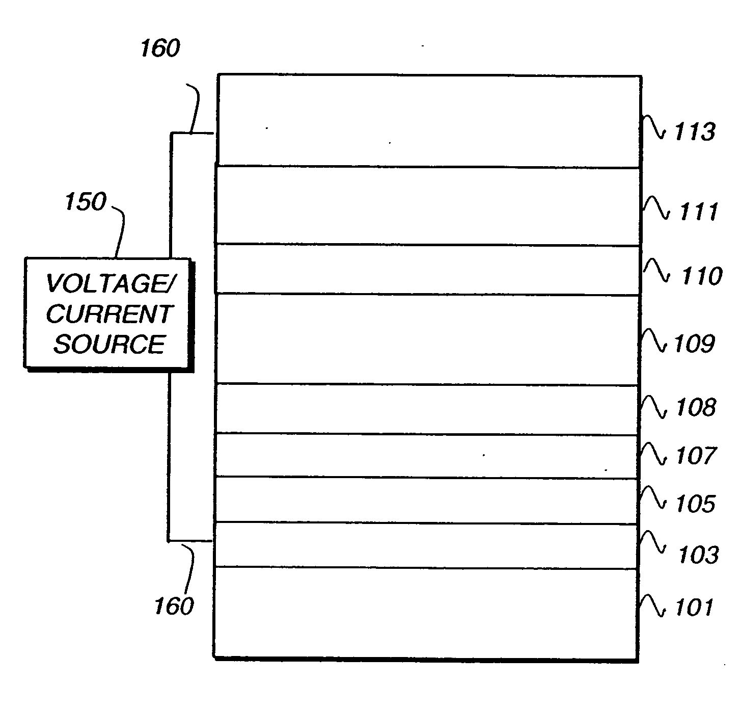
[0013] The invention provides an OLED device comprising a cathode, an anode, and having therebetween a light-emitting layer containing a phosphorescent emitter and a host comprising a first aluminum or gallium complex containing at least one 2-(2-hydroxyphenyl)pyridine ligand and at least one phenoxy ligand, wherein there is further present adjacent to the light-emitting layer on the cathode side a layer containing a second aluminum or gallium complex containing at least one 2-(2-hydroxyphenyl)pyridine ligand and at least one phenoxy ligand.
[0014] In one embodiment the first complex is an aluminum complex. In addition it is possible for the first and second complexes to be the same compound. The emitter in the light-emitting layer may be an iridium phosphorescent emitter.
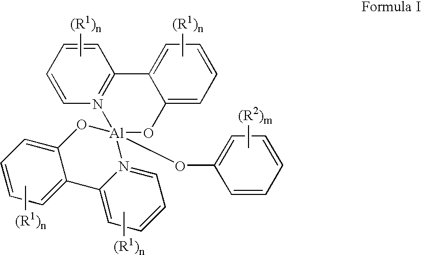
[0015] Suitably, the first complex is represented by Formula I:
wherein; R1 and R2 are independently selected from alkyl, aryl, heteroaryl, halogen, aryl amine, alkyl amine, and cyano groups, provided that group...
embodiment b
[0021] In another embodiment, the OLED devices comprises a cathode, an anode, and having therebetween a light-emitting layer containing a phosphorescent emitter and a host comprising a first aluminum or gallium complex containing at least one 2-(2-hydroxyphenyl)pyridine ligand and at least one phenoxy ligand substituted with an amine. The emitter in the light-emitting layer may be an iridium phosphorescent emitter. Suitably, the amine is selected from pyridine, pyrrole, and indole.
[0022] In one embodiment, the first complex is represented by Formula IV:
wherein; R1 and R2 are independently selected from alkyl, aryl, heteroaryl, halogen, aryl amine, alkyl amine, and cyano groups, provided that groups may join together to form fused rings; n is independently 0 to 4; and m is independently 0 to 5.
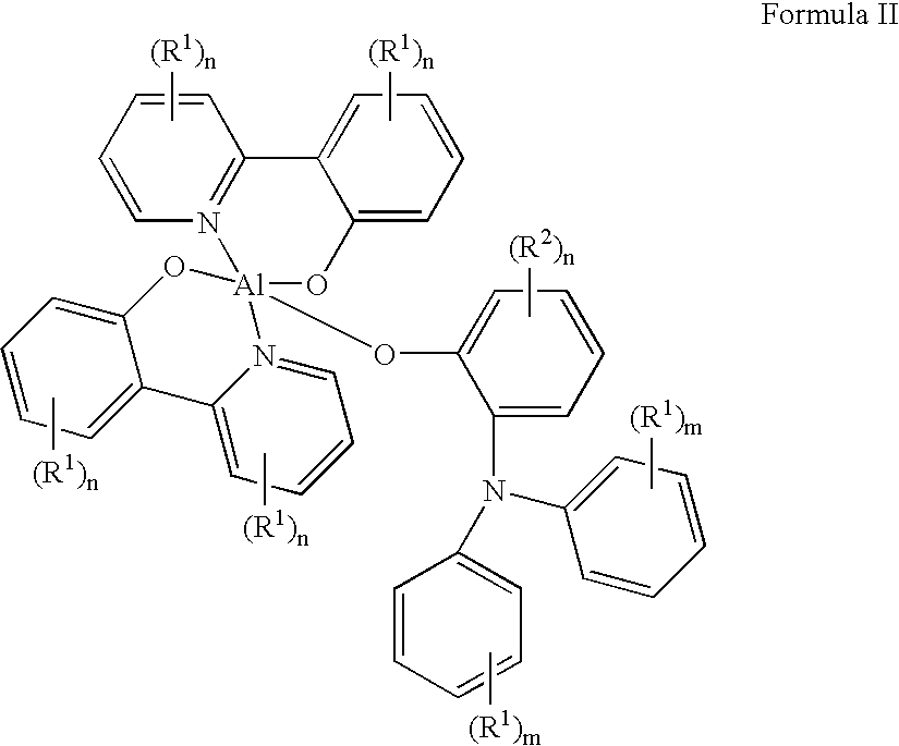
[0023] In a preferred embodiment the first complex is represented by Formula II:
wherein; R1 and R2 are independently selected from alkyl, aryl, heteroaryl, halogen, aryl amine, alkyl am...
example 1
[0278] An EL device satisfying the requirements of the invention was constructed in the following manner: [0279] 1. A glass substrate coated with an 85 nm layer of indium-tin oxide (ITO) as the anode was sequentially ultrasonicated in a commercial detergent, rinsed in deionized water, degreased in toluene vapor and exposed to oxygen plasma for about 1 min. [0280] 2. Over the ITO was deposited a 1 nm fluorocarbon (CFx) hole-injecting layer (HIL) by plasma-assisted deposition of CHF3. [0281] 3. A hole-transporting layer (HTL) of N,N′-di-1-naphthyl-N,N′-diphenyl-4,4′-diaminobiphenyl (NPB) having a thickness of 75 nm was then evaporated from a tantalum boat. [0282] 4. A 35 nm light-emitting layer (LEL) of Inv-2 and fac-tris(2-phenyl-pyridinato-NˆC-)Iridium(III) (Ir(ppy)3) (6 wt %) were then deposited onto the hole-transporting layer. These materials were also evaporated from tantalum boats. [0283] 5. A hole-blocking layer of Inv-2 having a thickness of 10 nm was then evaporated from a t...
PUM
| Property | Measurement | Unit |
|---|---|---|
| Electric potential / voltage | aaaaa | aaaaa |
| Electric potential / voltage | aaaaa | aaaaa |
| Electric potential / voltage | aaaaa | aaaaa |
Abstract
Description
Claims
Application Information