Organic electroluminescent devices

a technology of electroluminescent devices and electroluminescent tubes, which is applied in the direction of discharge tube luminescnet screens, natural mineral layered products, transportation and packaging, etc., can solve the problems of limited layer thickness, poor storage stability, and only able to deposit substantially all of the exemplified metal oxide compounds, so as to reduce the driving voltage and maintain the driving durability stability , the effect of diminishing the formation of the hole transfer barrier

Inactive Publication Date: 2005-05-19
ROHM CO LTD
View PDF13 Cites 180 Cited by
  • Summary
  • Abstract
  • Description
  • Claims
  • Application Information

AI Technical Summary

Benefits of technology

[0027] First, the hole injection layer with the mixed Lewis acid compound, suggested by the assignee of the present invention, is characterized by a driving voltage of an organic EL device not increasing with substantial increase of the thickness of the hole injection layer because of the low resistivity of the hole injection layer, and thus the hole injection layer is considered to be effective. On the other hand, generally, typical Lewis acid compounds are chemically instable and therefore they have poor storage stability. Furthermore, as a result of study, the inventors of the present invention have found that the Lewis acid compounds may slightly deteriorate the current efficiency (or quantum efficiency) of the organic EL device, while being able to reduce the driving voltage.
[0029] The hole injection layer using an organic compound having a small ionization potential, typically CuPc suggested by Tang et al., and an starburst type arylamine compound, for example, m-MTDATA, suggested by Shirota et al., can improve the contacting property at the anode electrode layer interface. However, due to such an upper limit for the layer thickness applicable to the formation of the hole injection layer, it is difficult to freely change the design of an organic EL device. Furthermore, it is essential for CuPc and the starburst type arylamine compound to be used as a hole injection layer adjacent to the anode electrode layer as in other hole injection layers, and that another hole transporting layer consisting of the organic compound having the different structures is further inserted between the hole injection layer and the luminous layer.
[0032] The formation or presence of such a hole transfer barrier are observed with the resulting increase of the driving voltage and the turn-on voltage, and of course, the increase of these voltages can result in reduction in the light emission efficiency (Im / W). Regardless of these circumstances, the CuPc and starburst type arylamine compounds are widely used as an excellent hole-injecting compound at present, because they can exhibit an excellent hole injection characteristic from the anode electrode layer, and also can exhibit an excellent thermal stability and layer formation stability, thereby remarkably improving a driving stability of organic EL devices.
[0033] In addition, among the various hole injection layers discussed above, the hole injection layer in the form of a mixed layer consisting of the metal oxide, V2O5 (vanadium pentoxide) or the like and the organic hole-transporting compound, arylamine compound, developed by the assignee of the present invention is one of the most effective hole injection layers, because it ensures advantages such as low resistivity, reduction in the barrier of the hole injection from the anode electrode layer and the above-described chemical stability. However, the inventors have studied and found in the driving durability test of the organic EL devices that the initial deterioration curve is somewhat steep, and thus the half-decay life of luminance is rather shortened in comparison with organic EL devices of the present invention which will be described hereinafter in detail.
[0035] Furthermore, the present invention maintains driving durability stability in an organic EL device by using a combination of two or more hole transportation layers for transferring holes injected from an anode electrode layer to a luminous layer (At present, typical examples of the combination include “CuPc and NPB”, “m-MTDATA and TPD” and “IDE406 and IDE312”, described above, and other combinations include a combination of the conductive polymer such as PEDOT and PANI and the arylamine compound), and at the same time, solves the problems caused by using the combination of the hole transportation layers, i.e., to diminish a formation of a hole transfer barrier in an interface of the hole transportation layers constituted from different organic molecules so that a device driving voltage including an turn on voltage is lowered as a result, thereby reducing a power consumption.
[0036] In particular, the present invention simultaneously reduces the driving voltage and stabilizes the device driving in the organic EL device by forming a hole transportation layer as a combination of two or more hole transportation layers as in the prior art organic EL devices, but applying an electron-accepting material near an interface separating the hole transportation layers and also forming a charge transfer complex upon the oxidation-reduction reaction between the electron-accepting material and either or both of the two hole-transporting materials contacting the electron-accepting material, thereby converting the hole-transporting materials to a radical cation state and thus diminishing the formation of the hole transfer barrier, which could not be solved in the prior art organic EL devices.

Problems solved by technology

On the other hand, generally, typical Lewis acid compounds are chemically instable and therefore they have poor storage stability.
The lamination of a metal oxide having a large work function on the anode electrode layer, suggested by Toyota Central R&D Labs., Inc., has a limited applicable layer thickness due to low light transmittance of the metal oxide.
Moreover, substantially all of the exemplified metal oxide compounds can only be deposited by a sputtering method to form a layer.
However, due to such an upper limit for the layer thickness applicable to the formation of the hole injection layer, it is difficult to freely change the design of an organic EL device.

Method used


Image

  • Organic electroluminescent devices
  • Organic electroluminescent devices
  • Organic electroluminescent devices

Examples


reference example 1

Production of Conventional Organic EL Device Using CuPc

[0127] The organic EL device having a lamination structure illustrated in FIG. 7 was produced as Reference Example 1.

[0128] The glass substrate 701 used in this example includes, as a transparent anode electrode (anode electrode layer) 702, a coating of ITO (indium-tin oxide; Nippon Sheet Glass Co., Ltd.) having a sheet resistance of about 10 Ω / □ (10 Ω / sq). Onto the ITO-coated glass substrate 701 was deposited CuPc represented by the following formula:

under vacuum of about 10−6 Torr and at the deposition rate of about 2 Å / sec to form a first hole transportation layer (hole injection layer) 711 having a thickness of about 150 Å.

[0129] Thereafter, onto the first hole transportation layer (hole injection layer) 711 was deposited Alpha(α)-NPD having a hole transporting property under vacuum of about 10−6 Torr and at a deposition rate of about 2 Å / sec to form a second hole transportation layer 712 having a thickness of about 5...

example 1

Production of Organic EL Device According to Present Invention

[0132] The organic EL device having a lamination structure illustrated in FIG. 8 was produced as Example 1.

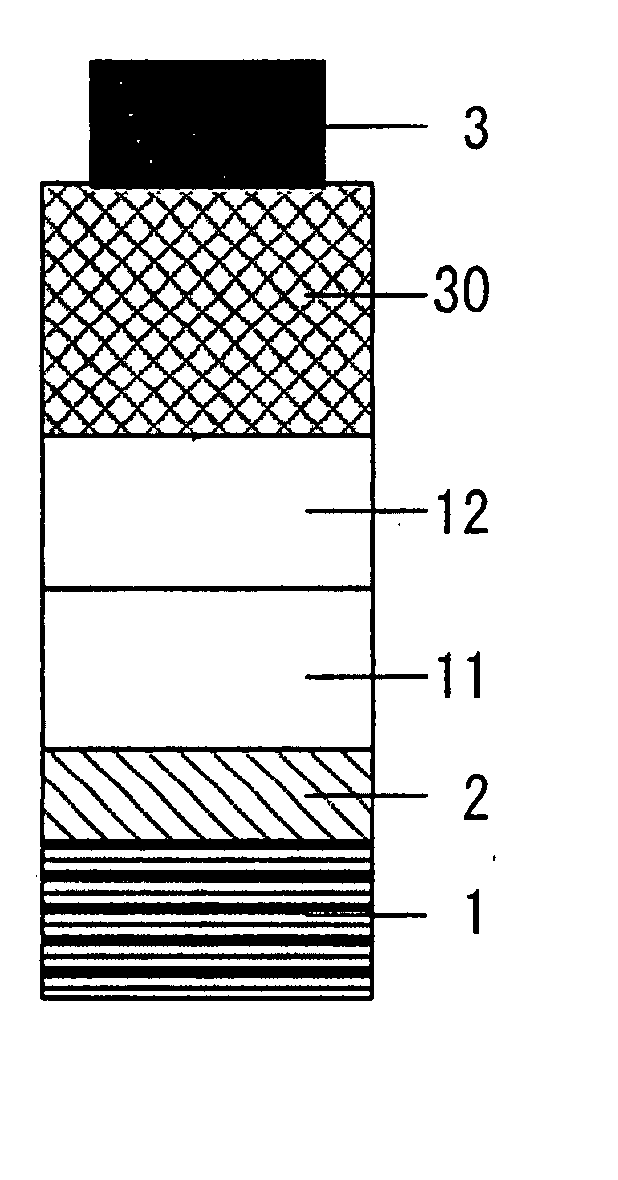
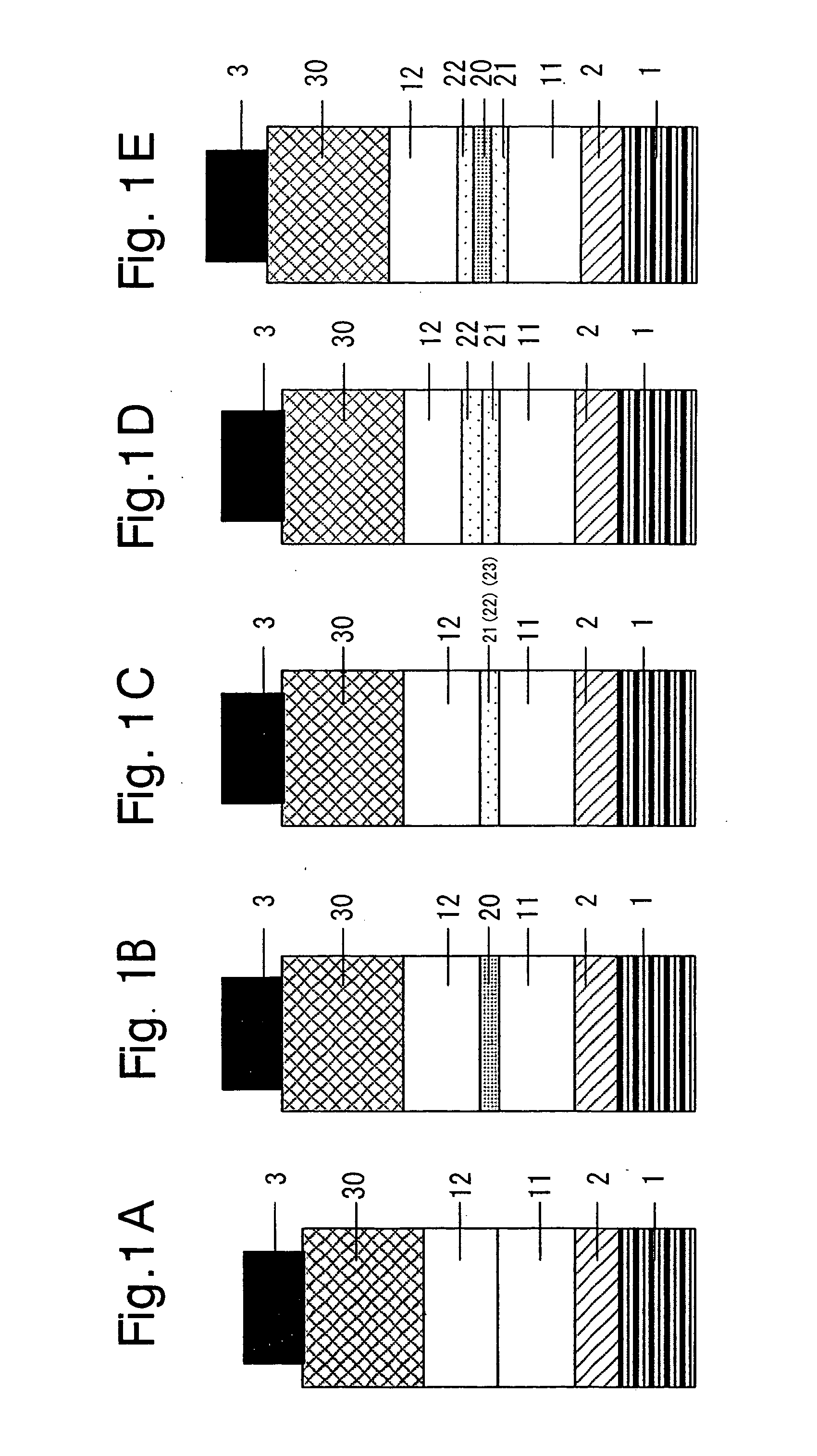
[0133] A glass substrate 801 used in this example includes, as a transparent anode electrode (anode electrode layer) 802, a coating of ITO (indium-tin oxide; Nippon Sheet Glass Co., Ltd.) having a sheet resistance of about 10 Ω / □. Onto the ITO-coated glass substrate 801 was deposited CuPc under conditions similar to those applied in Reference Example 1 to form a first hole transportation layer 811 having a thickness of about 150 Å. Subsequently, an electron-accepting material, V2O5 (vanadium pentoxide), which is one constitutional element of the present invention, and α-NPD, which is a constitutional material of the second hole transportation layer 802, were co-deposited at a molar ratio (V2O5: α-NPD) of about 4:1 on the first hole transportation layer 811 to form a mixed layer 822 having a thickness of about 100 ...

reference example 2

Production of Conventional Organic EL Device Using 2-TNATA

[0135] The organic EL device having a lamination structure illustrated in FIG. 9 was produced as Reference Example 2. The structure of the organic EL device is similar to that of Reference Example 1 except that the CuPc layer (150 Å) used as the first hole transportation layer in Reference Example 1 was replaced with a 2-TNATA layer (600 Å), described above.

[0136] Namely, a transparent anode electrode (ITO) 902, a first hole transportation layer (2-TNATA) 911, a second hole transportation layer (α-NPD) 912, a luminous layer (Alq) 906, an electron injection layer (Liq) 907 and a cathode electrode layer (903) were deposited, in sequence, on the glass substrate 901 in accordance with the manner described in Reference Example 1 to form an organic EL device.

[0137] In the resulting organic EL device, a DC voltage was applied between ITO (transparent anode electrode 902) and Al (cathode electrode layer 903), and the luminance of...


PUM

PropertyMeasurementUnit
thicknessaaaaaaaaaa
external quantum efficiencyaaaaaaaaaa
luminanceaaaaaaaaaa

Abstract

An organic electroluminescent device includes an anode electrode layer, a cathode electrode layer opposed to the anode electrode layer, and a luminous layer containing an organic compound disposed between the anode electrode layer and the cathode electrode layer. An excitation state of the organic compound in the luminous layer is created upon a hole injection from the anode electrode layer, and an electron injection from the cathode electrode layer, thereby causing light emission in the organic electroluminescent device. An electron-accepting material is provided in at least one hole transportation layer capable of transporting holes injected from the anode electrode layer disposed between the anode electrode layer and the cathode electrode layer, and the electron-accepting material is positioned at a site which is not adjacent to the anode electrode layer.

Description

CROSS REFERENCE TO RELATED APPLICATIONS [0001] The present application is related to and claims priority of the following priority applications, namely, Japanese Patent Application Nos. 2003-384202 filed on Nov. 13, 2003, and 2004-309943 filed on Oct. 25, 2004, and incorporates by reference said priority applications herein. BACKGROUND OF THE INVENTION [0002] 1. Field of the Invention [0003] The present invention relates to an organic electroluminescent device (organic EL device) used as a planar light source or as a display device. [0004] 2. Description of the Related Art [0005] A great deal of interest has been directed toward organic EL devices in which a luminous layer thereof is constructed from an organic compound, due to being able to ensure a large area display at a low driving voltage. [0006] To significantly increase the efficiency of organic EL devices, Tang et al. of Eastman Kodak Company, as is reported in Appl. Phys. Lett., 51, 913 (1987), have successfully achieved an...

Claims


Application Information

Patent Timeline
Patent Type & Authority Applications(United States)
IPC IPC(8): C09K11/06H05B33/26H01L51/00H01L51/10H01L51/30H01L51/50H01L51/52H05B33/00
CPCH01L51/0051H01L51/0052H01L51/0059H01L51/0077Y10T428/24942H01L51/0081H01L51/5048H01L51/5278H01L51/0078H10K85/611H10K85/615H10K85/631H10K85/311H10K85/30H10K85/324H10K50/14H10K50/19H05B33/26
Inventor ENDOH, JUNKIDO, JUNJI
Owner ROHM CO LTD
Why Eureka
Try Eureka