Method for preparing high-uniformity Nb-doped TiO2 transparent conducting thin film through atomic layer deposition

A technology of transparent conductive thin film and atomic layer deposition, which is applied in the direction of coating, metal material coating process, gaseous chemical plating, etc. Process parameters are easy to control, reduce experimental conditions and energy consumption, and achieve high uniformity

Active Publication Date: 2016-10-12
SHANGHAI NAT ENG RES CENT FORNANOTECH
View PDF2 Cites 123 Cited by
  • Summary
  • Abstract
  • Description
  • Claims
  • Application Information

AI Technical Summary

Problems solved by technology

[0003] Nb doped TiO 2 It is one of the most concerned titanium dioxide-based transparent conductive materials. Researchers have deposited it through electron beam deposition (Thin Solid Films, 525(15) 28–34, 2012), sol-gel (Ceramics International, 39(5), 4771 –4776) and hydrothermal method (Journal of Materials Chemistry A, 3(45)

Method used


Image

  • Method for preparing high-uniformity Nb-doped TiO2 transparent conducting thin film through atomic layer deposition
  • Method for preparing high-uniformity Nb-doped TiO2 transparent conducting thin film through atomic layer deposition

Examples


Embodiment 1

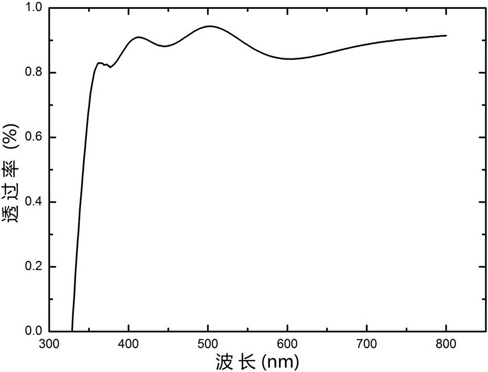
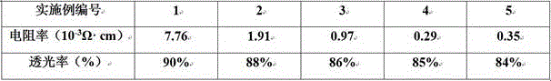
[0024] Load titanium tetrachloride, niobium tris(ethylmethylamino) tert-butyramide and high-purity water source on the machine, set the temperature of niobium tris(ethylmethylamino) tert-butyramide to 55°C; when the deposition chamber After heating to 200°C, place the glass substrate after ultrasonic cleaning with alcohol, acetone and deionized water in the deposition chamber; after vacuuming to 15hPa, perform TiO 2 cycle; that is, titanium tetrachloride / nitrogen / water / nitrogen = (0.4s / 6s / 0.2s / 4s); after 49 cycles, a niobium doping cycle is performed, that is, titanium tetrachloride / nitrogen / tri(B Base methyl amino) niobium tert-butyramide / nitrogen / water / nitrogen = (0.4s / 6s / 0.6s / 8s / 0.2s / 4s); the deposition is combined into a set of cycles, and this set of cycles is carried out for 40 groups; end Finally, the sample was taken out to make a Nb-doped TiO with a thickness of about 100nm. 2 film. After EDS mapping composition, the doping amount of Nb is about 0.65at.%; at this ti...

Embodiment 2

[0026] Load titanium tetrachloride, niobium tris(ethylmethylamino) tert-butyramide and high-purity water source on the machine, set the temperature of niobium tris(ethylmethylamino) tert-butyramide to 55°C; when the deposition chamber After heating to 220°C, place the glass substrate after ultrasonic cleaning with alcohol, acetone and deionized water in the deposition chamber; after vacuuming to 15hPa, perform TiO 2cycle; that is, titanium tetrachloride / nitrogen / water / nitrogen = (0.4s / 6s / 0.2s / 4s); after 24 cycles, a niobium doping cycle is performed, that is, titanium tetrachloride / nitrogen / tri(B Base methyl amino) niobium tert-butyramide / nitrogen / water / nitrogen = (0.4s / 6s / 0.6s / 8s / 0.2s / 4s); the deposition is combined into a set of cycles, and the set of cycles is carried out for 80 groups; end Finally, the sample was taken out to make a Nb-doped TiO with a thickness of about 100nm. 2 film. After EDS mapping composition, the doping amount of Nb is about 1.31at.%; at this time...

Embodiment 3

[0028] Load titanium tetrachloride, niobium tris(ethylmethylamino) tert-butyramide and high-purity water source on the machine, set the temperature of niobium tris(ethylmethylamino) tert-butyramide to 55°C; when the deposition chamber After heating to 240°C, place the glass substrate after ultrasonic cleaning with alcohol, acetone and deionized water in the deposition chamber; after vacuuming to 15hPa, perform TiO 2 cycle; that is, titanium tetrachloride / nitrogen / water / nitrogen = (0.4s / 6s / 0.2s / 4s); after 19 cycles, a niobium doping cycle is performed, that is, titanium tetrachloride / nitrogen / tri(B Base methyl amino) niobium tert-butyramide / nitrogen / water / nitrogen = (0.4s / 6s / 0.6s / 8s / 0.2s / 4s); the deposition is combined into a set of cycles, and the set of cycles is carried out for 100 groups; end Finally, the sample was taken out to make a Nb-doped TiO with a thickness of about 100nm. 2 film. According to the EDS mapping composition, the Nb doping amount is about 1.65 at.%; a...


PUM


Abstract

The invention relates to a method for preparing a high-uniformity Nb-doped TiO2 transparent conducting thin film through atomic layer deposition in the technical field of semiconductor photoelectric materials. According to the method, a substrate which is subjected to ultrasonic cleaning and nitrogen blowing-drying is heated; titanium tetrachloride, niobium tris(ethylmethylamido)-tert-butylimino and high purity water serve as precursor sources; and deposition combination is cycled for multiple times, so that the high-uniformity Nb-doped TiO2 transparent conducting thin film is prepared. The transparent conducting thin film prepared through the method is excellent in performance; the refractive index is 2.3 or above; the electrical resistivity can reach 2.9*10<4> omega.cm at a minimum; and at this moment, the light transmittance is still 85% or above.

Description

technical field [0001] The invention belongs to the field of semiconductor photoelectric material preparation, in particular to metal Nb doped TiO 2 Atomic layer deposition preparation method of transparent conductive thin film. Through atomic layer composite deposition, it is possible to precisely control the doping uniformity of metal niobium, control the doping content and film thickness, and obtain TiO with significantly improved photoelectric performance. 2 base transparent conductive film. Background technique [0002] Transparent conducting films (Transparent conducting films) have a wide range of applications in the semiconductor industry due to their good optical and electrical properties, such as liquid crystal displays, micro-electromechanical systems, solar cells, and light-emitting diodes. In previous studies, indium-doped tin oxide (ITO) and aluminum-doped zinc oxide (ZAO) have been widely used. However, the above materials still have many limitations: for e...

Claims


Application Information

Patent Timeline
IPC IPC(8): C23C16/40C23C16/455
CPCC23C16/405C23C16/45529
Inventor 何丹农卢静张彦鹏尹桂林葛美英金彩虹
Owner SHANGHAI NAT ENG RES CENT FORNANOTECH
Why Eureka
Try Eureka