

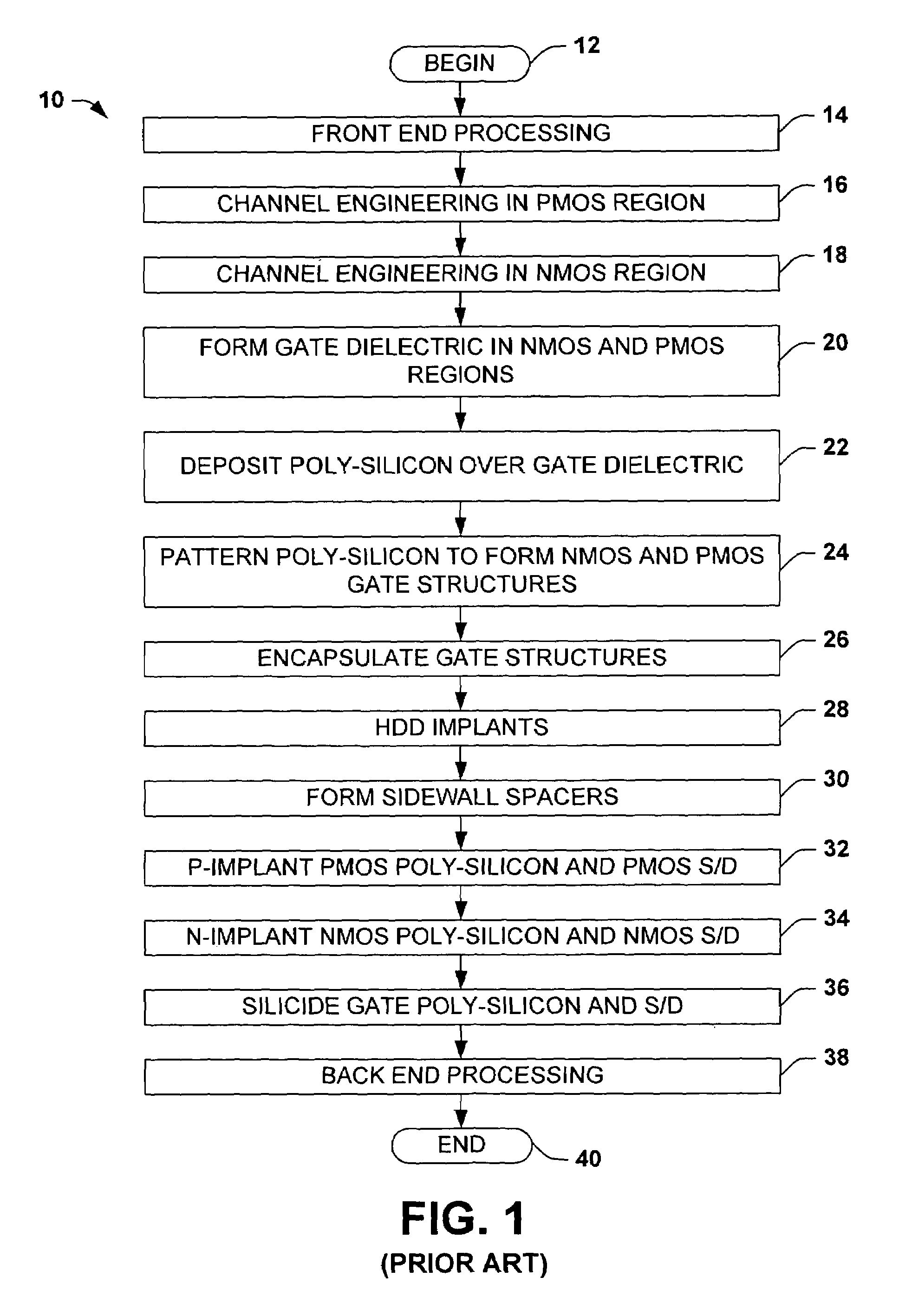
MOS transistor gates with thin lower metal silicide and methods for making the same
a technology of metal silicide and transistor, which is applied in the direction of transistors, semiconductor devices, electrical equipment, etc., can solve the problems of gate leakage current tunneling through, limited ability to form very thin oxide films with uniform thickness, and inability to so as to prevent undesired silicidation, inhibit oxidation or other degradation of the first metal, and reduce the composition of the silicid
- Summary
- Abstract
- Description
- Claims
- Application Information
AI Technical Summary
Benefits of technology
Problems solved by technology
Method used
Image

Examples
Embodiment Construction
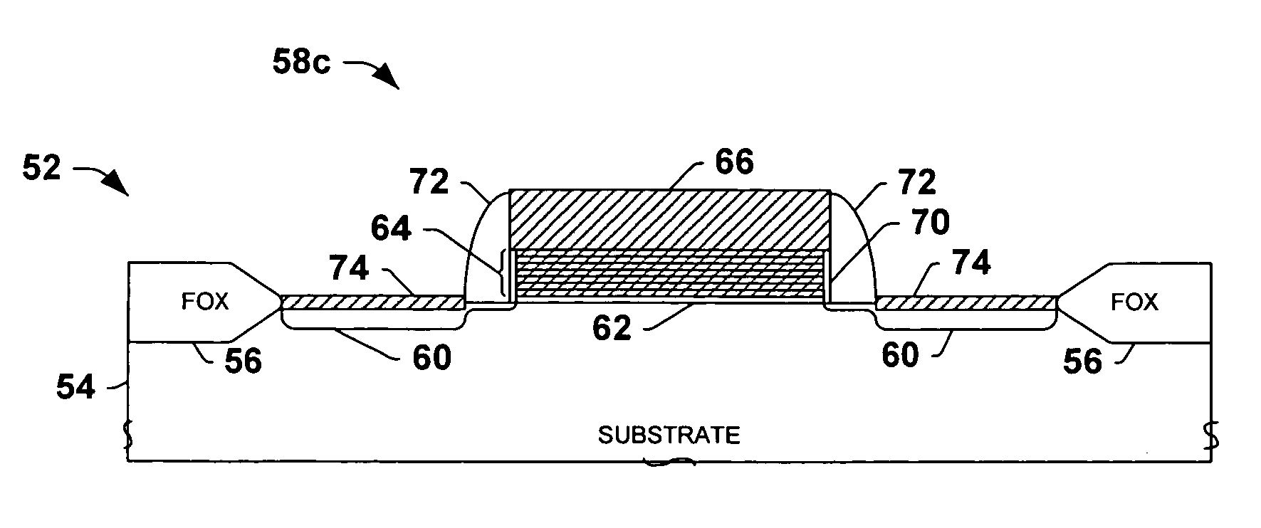
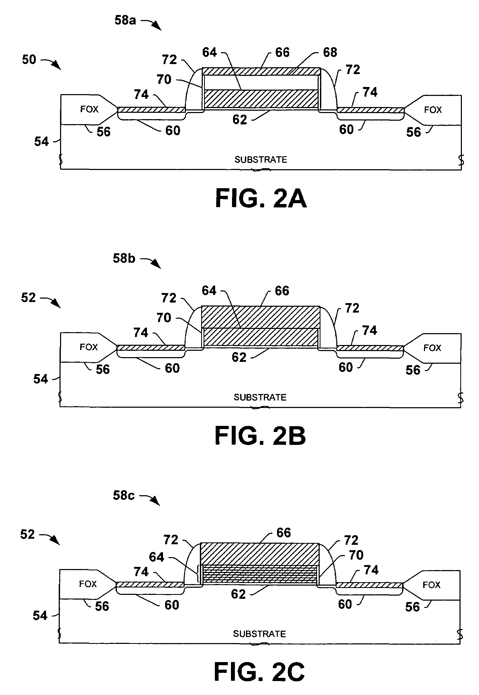
[0026]One or more implementations of the present invention will now be described with reference to the attached drawings, wherein like reference numerals are used to refer to like elements throughout, and wherein the illustrated structures are not necessarily drawn to scale. The invention relates to transistor gate structures and fabrication methods therefor, in which two or more suicides are used to form the gate electrode or gate contact. Several implementations of the invention are hereinafter illustrated and described in which a first or lower metal silicide is formed using polysilicon and a refractory metal, either as a single first suicide or a multilayer lower silicide stack structure. However, any silicon-containing materials and metals may be employed in creating metal silicide materials, wherein the invention is not limited to the specific materials and structures illustrated and described herein.
[0027]FIGS. 2A–2C illustrate exemplary CMOS semiconductor devices 50 and 52, ...
PUM
| Property | Measurement | Unit |
|---|---|---|
| thickness | aaaaa | aaaaa |
| refractory | aaaaa | aaaaa |
| electric field | aaaaa | aaaaa |
Abstract
Description
Claims
Application Information