Actively driven organic EL device and manufacturing method thereof

a technology of organic el and light emission, which is applied in the direction of identification means, semiconductor/solid-state device details, instruments, etc., can solve the problems of small aperture ratio of pixels (the proportion of parts) and drop in luminous efficiency or power consumption, and achieve low sheet resistivity of upper electrodes and large apertures.

Inactive Publication Date: 2005-08-23
IDEMITSU KOSAN CO LTD
View PDF19 Cites 116 Cited by
  • Summary
  • Abstract
  • Description
  • Claims
  • Application Information

AI Technical Summary

Benefits of technology

[0034]Such a structure makes it possible to make a numerical aperture large even if a TFT is set up and make the sheet resistivity of the upper electrode reduced even if luminescence is taken out from the side of the upper electrode.
[0073]According to such an embodiment, it is possible to provide an active-driving organic EL light emission device wherein numerical aperture is large even if the TFT is disposed and further the sheet resistivity of the upper electrode is low even if luminescence is taken out from the side of the upper electrode.

Problems solved by technology

(1) Since a driving voltage becomes not less than 2-3 times higher than a direct-current constant voltage, luminous efficiency drops or power consumption becomes large.
Accordingly, there arises a problem that when light is taken out from the side of the transparent substrate, the aperture ratio of the pixels (the ratio of portions that emits light actually in the pixels) becomes small since the TFTs and the various electrode lines shut off the light.
As a result, dependently on the aperture ratio, the current density that passes through the organic luminous medium becomes large, causing a problem that the life span of the organic EL elements is shortened.
For this reason, the sheet resistivity of the upper electrodes exceeds, for example, 20 Ω / □, resulting in a serious problem at the time of using large-area display.
Thus, it is difficult to emit light under the above-mentioned conditions.
As a result, a problem that brightness is remarkably lowered becomes apparent.
However, this attempt is insufficient.
(3) From the viewpoint of production, it is difficult to control the ohmic value of the upper electrodes.
As a result, a problem that the sheet resistivity becomes a high value over 20 Ω / □ occurs.
In the case that plasma is used for sputtering at the time of forming an oxide such as ITO or IZO on the organic luminous medium to form the upper electrodes, a problem that the organic luminous medium is damaged by the plasma also arises.

Method used


Image

  • Actively driven organic EL device and manufacturing method thereof
  • Actively driven organic EL device and manufacturing method thereof
  • Actively driven organic EL device and manufacturing method thereof

Examples


first embodiment

[First Embodiment]

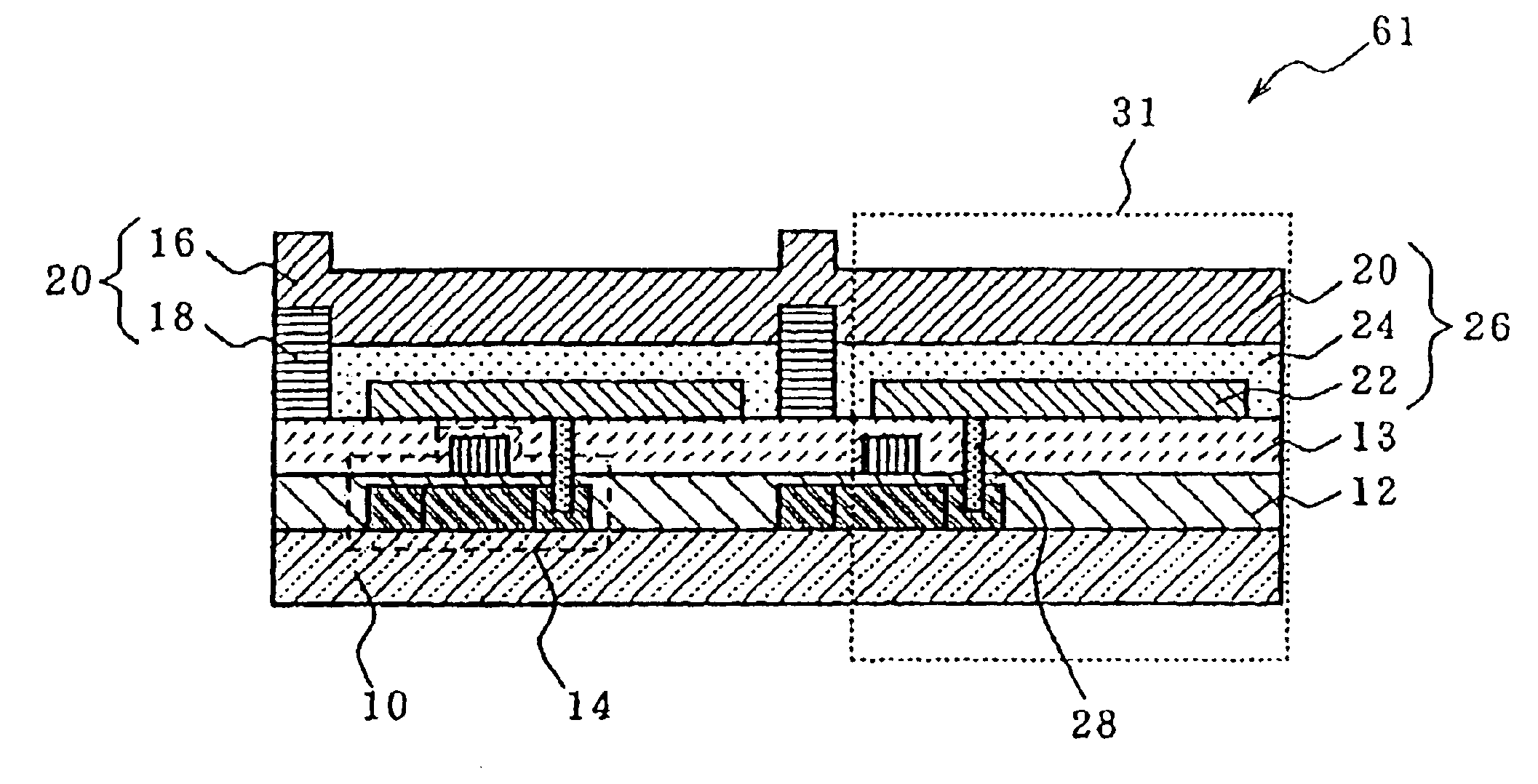
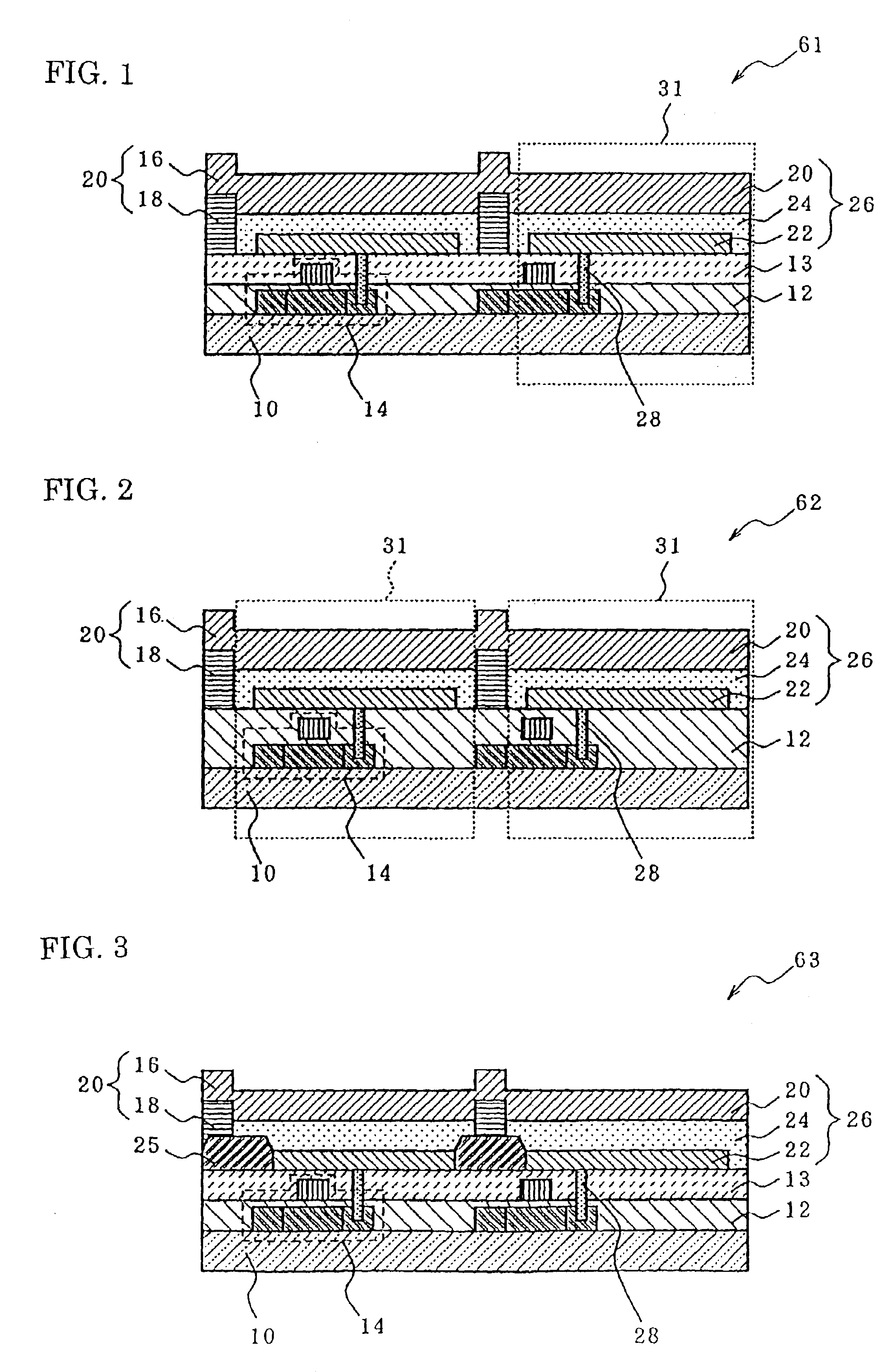
[0094]As illustrated in FIG. 1, an active-driving organic EL light emission device of a first embodiment is an active-driving organic EL light emission device 61 having, on a substrate 10, TFTs 14 embedded in an electrically insulating film 12, an interlayer insulating film (flattening film) 13 deposited on the TFTs 14, organic EL elements 26, each of which comprises an organic luminous medium 24 between an upper electrode 20 and a lower electrode 22, and electric connecting portions 28 for connecting the TFT 14 with the organic EL element 26.

[0095]In order to take out luminescence (EL light) of the organic element 26 and make the resistance of the upper electrode 20 low in the first embodiment, the upper electrode 20 comprises a main electrode 16 made of transparent conductive material and an auxiliary electrode 18 made of low-resistance material.

[0096]The following will describe constituent elements of the first embodiment, and the like, referring appropriately t...

second embodiment

[Second Embodiment]

[0207]As shown in FIG. 5, the active-driving organic EL light emission device of the second embodiment is an active-driving organic EL light emission device 64 comprising, on the substrate 10, the TFT 14 embedded in the electrically insulating film 12, the organic EL element 26 comprising the organic luminous medium 24 between the upper electrode 20 and the lower electrode 22, and the electrically connecting portion (via hole) 28 for connecting the TFT 14 and the organic EL element 26 to each other.

[0208]The second embodiment is characterized in that, the upper electrode 20 is composed of the main electrode 16 and the auxiliary electrode 18, and further above the upper electrode 20 is set up a color filter or fluorescent film 60 for color-converting EL light taken out from the side of the upper electrode 20. (An arrow in FIG. 5 represents a direction along which the light is taken out.)

[0209]The following will describe the characteristic parts and the like of the ...

third embodiment

[Third Embodiment]

[0220]As shown in FIGS. 7 and 8, the active-driving organic EL light emission device 66 or 67 of a third embodiment comprises, on the substrate 10, the TFT 14 embedded in the electrically insulating film 12, the organic EL element 26 comprising the organic luminous medium 24 between the upper electrode 20 and the lower electrode 22, the electrically connecting portion 28 for connecting the TFT 14 and the organic EL element 26 electrically to each other, and a sealing member 58.

[0221]The third embodiment, wherein the upper electrode 20 comprises the main electrode 16 and the auxiliary electrode 18 and further the assistant element 18 in the upper electrode 20 is disposed in the state that it is embedded in the sealing member 58 and caused to penetrate through the sealing member 58 as shown in FIG. 7, or the assistant element 18 is arranged in the state that it is closely adhered to the sealing member 58 as shown in FIG. 8.

[0222]The following will describe the sealin...


PUM


Abstract

The present invention is a active-driving organic EL light emission device comprising an organic EL element comprising an organic luminous medium between an upper electrode and a lower electrode, and a thin film transistor for driving this organic EL element, wherein light emitted from the organic EL element is taken out from the side of the upper electrode, and the upper electrode comprises a main electrode formed of transparent conductive material, and an auxiliary electrode formed of a low-resistance material. According to the active-driving organic EL light emission device of this structure, the numerical aperture can be made large. Additionally, the sheet resistivity of the upper electrode can be made low even if luminescence is taken out from the side of the upper electrode. Thus, it is possible to provide an active-driving organic EL light emission device making it possible to display images having a high brightness and a homogenous brightness; and a method for manufacturing the same.

Description

[0001]This is a Continuation of application Ser. No. 09 / 784,0303 filed Feb. 16, 2001 now U.S. Pat. No. 6,538,374.BACKGROUND OF THE INVENTION[0002]1. Field of the Invention[0003]The present invention relates to an active-driving organic EL light emission device (which may be referred to merely as an organic EL device hereinafter) having a thin film transistor (which may be referred to as a TFT). More specifically, the present invention relates to an organic EL device used suitably for display equipment and color displays for the people's livelihood and industries, and the like.[0004]In the present specification, the description “EL” means “electroluminescence”.[0005]2. Description of the Related Art[0006]Conventionally, it is known a simple-driving organic EL light emission device which is simply driven by XY matrix electrodes to display an image (Japanese Patent Application Laid-Open (JP-A) No. 37385 / 1990, JP-A No. 233891 / 1991 and the like) as an organic EL light emission device (di...

Claims


Application Information

Patent Timeline
Patent Type & Authority Patents(United States)
IPC IPC(8): H05B33/28G09F9/00G09F9/30G09G3/30H01L27/32H01L51/50H01L51/52H05B33/00H05B33/10H05B33/12H05B33/14H05B33/26H05B44/00
CPCH05B33/12H10K59/122H10K59/12H10K59/1315H10K59/131H10K50/81H10K50/814H10K50/824H10K50/828H10K50/865H10K50/86H10K2102/3026H01L23/4855H10K50/82
Inventor HOSOKAWA, CHISHIO
Owner IDEMITSU KOSAN CO LTD
Why Eureka
Try Eureka