

Method of making a diode read/write memory cell in a programmed state
a memory cell and diode technology, applied in the field of nonvolatile memory arrays, can solve the problems of difficult fabrication and operation of three-terminal devices, difficult work of chalcogenides, complex solutions for achieving erasable or multi-state cells, etc., and achieve the effect of low resistivity
- Summary
- Abstract
- Description
- Claims
- Application Information
AI Technical Summary
Benefits of technology
Problems solved by technology
Method used
Image

Examples
Embodiment Construction
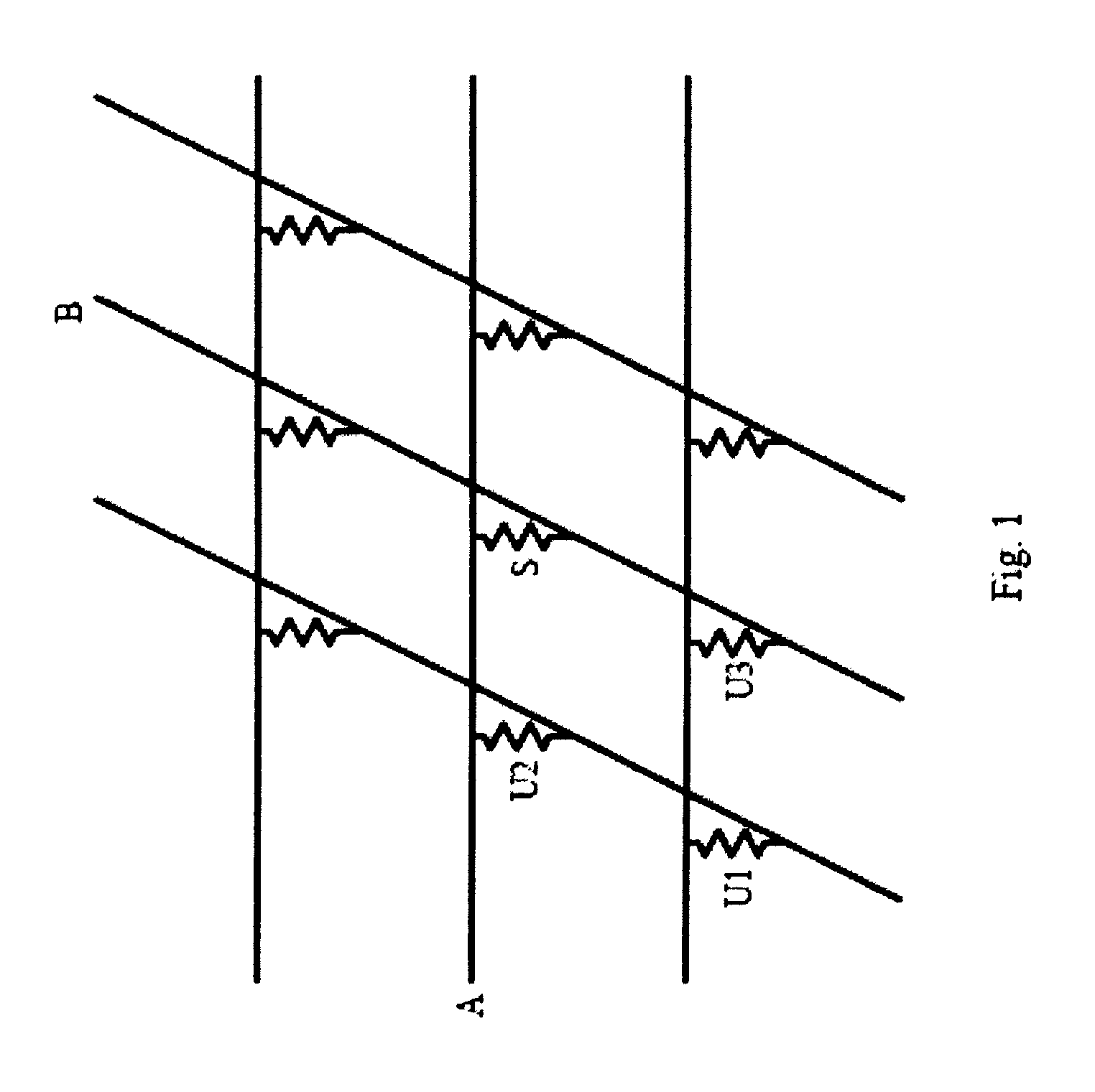
[0008] One embodiment of the invention provides a method of making a nonvolatile memory device comprising at least one memory cell which consists essentially of a diode and electrically conductive electrodes contacting the diode, the method comprising fabricating the diode in a low resistivity, programmed state without an electrical programming step.
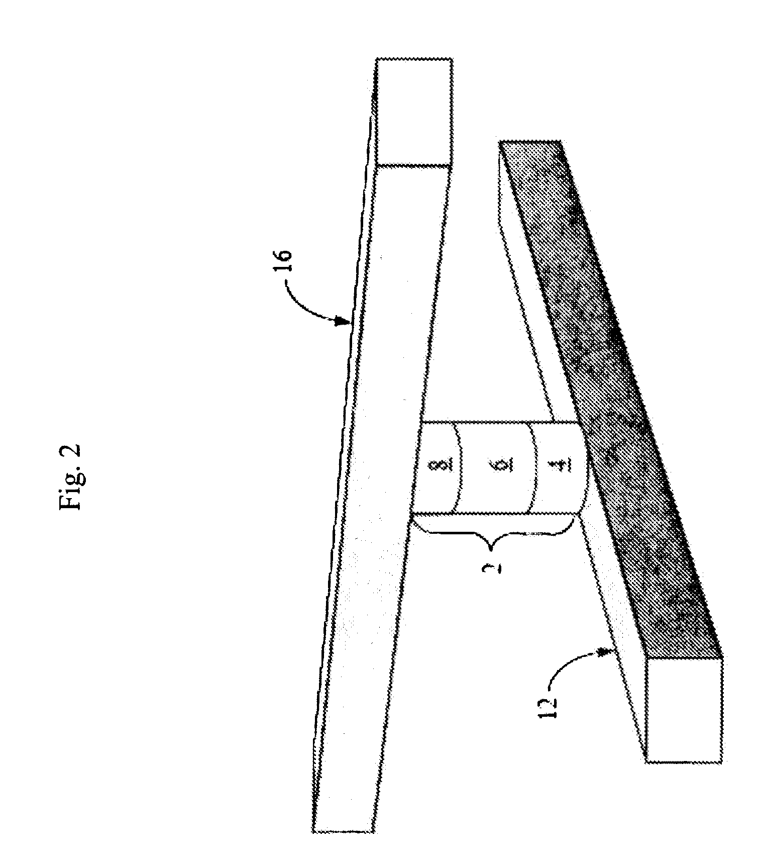
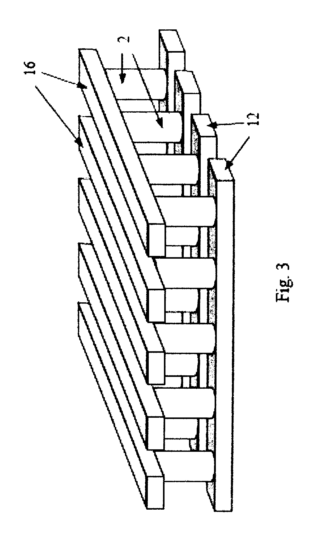
[0009] Another embodiment of the invention provides a method of making a diode, comprising forming a first electrode, forming a semiconductor region in electrical contact with the first electrode, wherein the semiconductor region comprises a p-n or a p-i-n junction in at least one silicon, germanium or silicon-germanium layer, forming a titanium layer on the semiconductor region, forming a titanium nitride layer on the titanium layer, reacting the titanium layer with the semiconductor region to form a titanium silicide, titanium germanide, or titanium silicide-germanide layer on the semiconductor region, removing the titanium nitride la...
PUM
 Abstract
Description
Claims
Application Information