Semiconductor optical modulator

a technology of optical modulator and semiconductor, applied in the direction of optical waveguide light guide, instruments, optics, etc., can solve the problems of large driving voltage, difficult difficulty in arranging input and output waveguides on the same side of the substrate, so as to reduce the size of the modulator, and reduce the length of the chirping

Inactive Publication Date: 2019-01-10
SUMITOMO ELECTRIC IND LTD
View PDF13 Cites 1 Cited by
  • Summary
  • Abstract
  • Description
  • Claims
  • Application Information

AI Technical Summary

Benefits of technology

[0004]In an optical communication system, QPSK is used as a method for transmitting 2-bit information by using four phases of signal light. Mach-Zehnder optical modulators are used to generate QPSK signal light. Such a modulator may include an electro-optic crystal of, for example, lithium niobate (LiNbO3), or a semiconductor such as GaAs or InP. A modulator including an electro-optic crystal is advantageous in that wavelength chirping can be reduced, but has a problem that a large driving voltage is required and it is difficult to reduce the size of the modulator. A modulator including a semiconductor is advantageous in that it is small and can be driven at a high speed and low driving voltage.

Problems solved by technology

A modulator including an electro-optic crystal is advantageous in that wavelength chirping can be reduced, but has a problem that a large driving voltage is required and it is difficult to reduce the size of the modulator.
When the two modulators are disposed close to each other on a single substrate to achieve size reduction, it is difficult to arrange input and output waveguides on the same side of the substrate if the modulators include arc-shaped waveguides that are bent 180°.

Method used


Image

  • Semiconductor optical modulator
  • Semiconductor optical modulator
  • Semiconductor optical modulator

Examples


Embodiment Construction

Description of Embodiments of the Invention

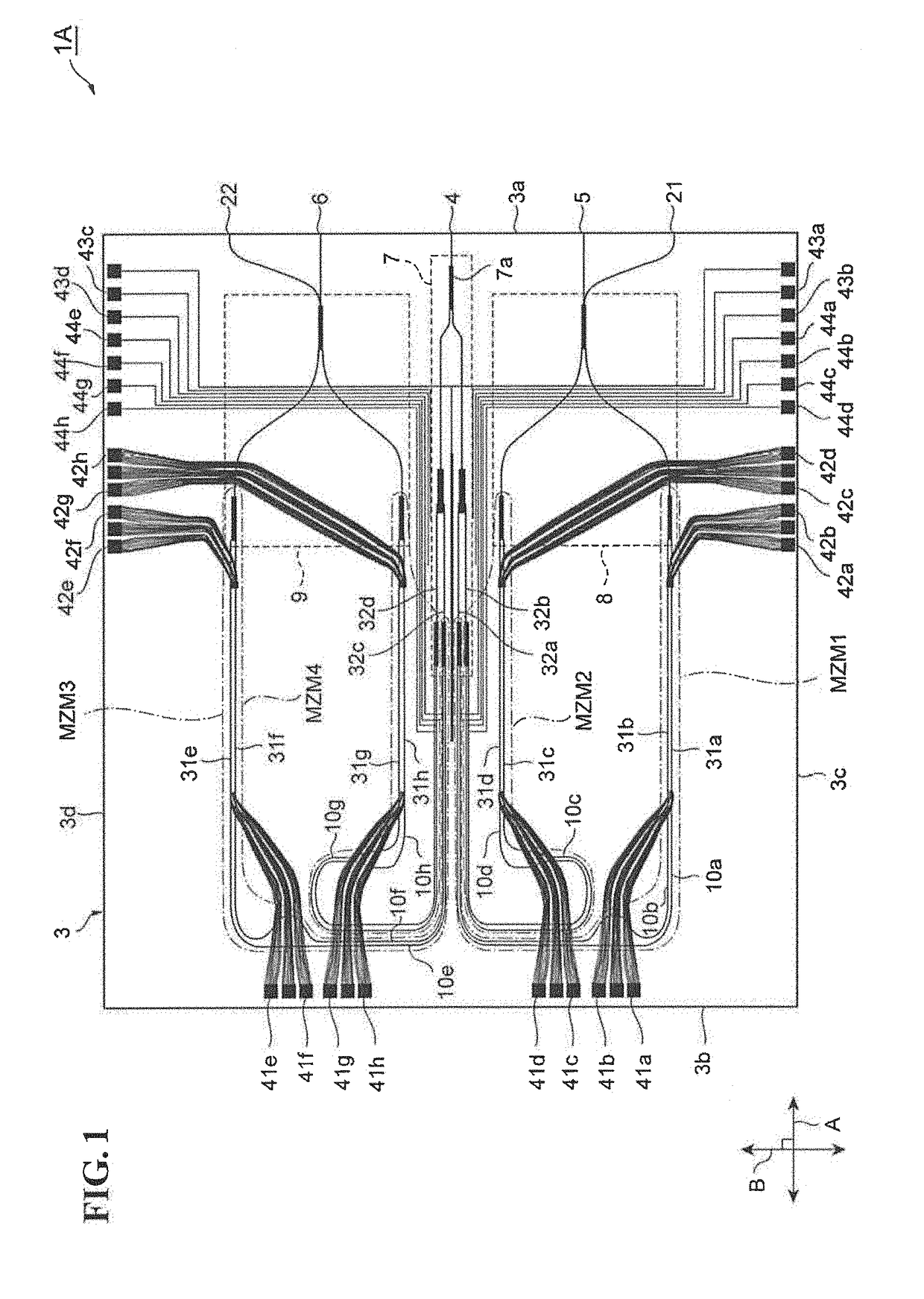
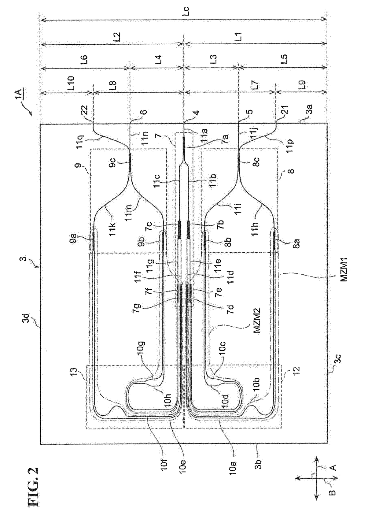
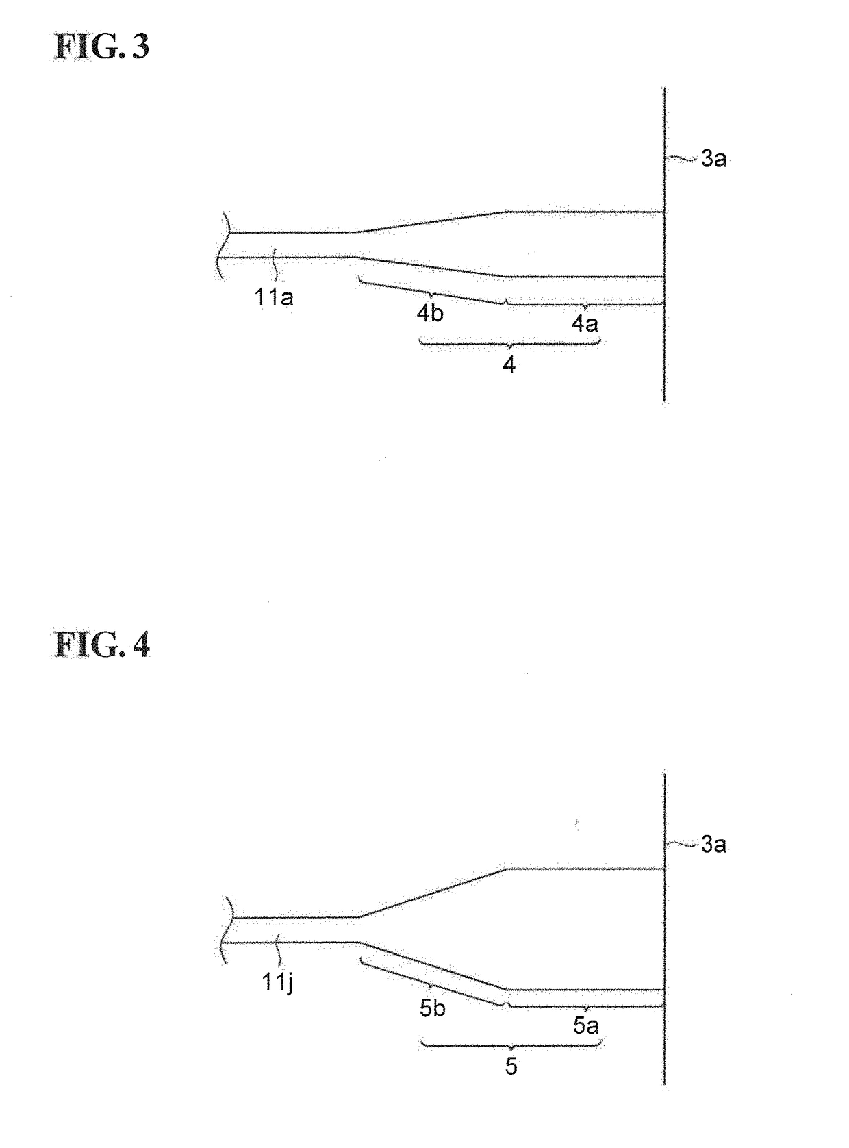
[0023]First, embodiments of the present invention will be described. A semiconductor optical modulator according to one embodiment includes an input waveguide provided on a side of a substrate; a first and second output waveguides provided on the side and arranged symmetrically about the input waveguide; a dividing portion optically connected to the input waveguide; eight arm waveguides, each arm waveguide being optically connected to the dividing portion; a first multiplexing portion optically connecting four of the arm waveguides to the first output waveguide; a second multiplexing portion optically connecting the other four of the arm waveguides to the second output waveguide; and modulation electrodes provided on respective ones of the eight arm waveguides.

[0024]In the above-described semiconductor optical modulator, the input waveguide and the two output waveguides are provided on the same side of the substrate. When this semiconductor...


PUM

PropertyMeasurementUnit
lengthaaaaaaaaaa
lengthaaaaaaaaaa
widthaaaaaaaaaa

Abstract

A semiconductor optical modulator includes an input waveguide provided on a side of a substrate, a first and a second output waveguides provided on the same side of the substrate, a dividing portion optically connected to the input waveguide, eight arm waveguides optically connected to the dividing portion, a first multiplexing portion optically connecting four of the arm waveguides to the first output waveguide, a second multiplexing portion optically connecting the other four of the arm waveguides to the second output waveguide, and modulation electrodes provided on respective ones of the eight arm waveguides. The first and second output waveguides are arranged symmetrically about the input waveguide.

Description

BACKGROUND OF THE INVENTION1. Field of the Invention[0001]The present invention relates to a semiconductor optical modulator.2. Description of the Related Art[0002]Japanese Unexamined Patent Application Publication No. 2009-229592, hereinafter referred to as Patent Document 1, describes a Mach-Zehnder optical modulator for use in polarization multiplex communication. This modulator includes an electro-optic crystal of, for example, lithium niobate or lithium tantalate. In this modulator, a λ / 4 plate and a mirror that are attached to an end of a rectangular substrate change the polarization mode of light that propagates through the modulator from a transverse magnetic (TM) mode to a transverse electric (TE) mode.[0003]Japanese Unexamined Patent Application Publication No. 2012-163876, hereinafter referred to as Patent Document 2, describes a modulator constituted by a Mach-Zehnder semiconductor and applied to quadrature phase shift keying (QPSK). This modulator includes a bent portio...

Claims


Application Information

Patent Timeline
Patent Type & Authority Applications(United States)
IPC IPC(8): G02F1/225
CPCG02F1/2257G02F2201/06G02F2201/58G02F2001/212G02F1/025G02F1/0356G02F1/212G02B6/12G02B6/125G02B2006/12119G02B2006/12142G02F1/0151G02F1/0154
Inventor KIKUCHI, TAKEHIKOKONO, NAOYA
Owner SUMITOMO ELECTRIC IND LTD
Why Eureka
Try Eureka