Display device and method of manufacturing a display device

Inactive Publication Date: 2018-12-06
JAPAN DISPLAY INC
View PDF5 Cites 0 Cited by
  • Summary
  • Abstract
  • Description
  • Claims
  • Application Information

AI Technical Summary

Benefits of technology

The present invention is aimed at providing a display device with an improved mounting mechanism for components to prevent mounting failure. The method involves placing a component on one side of a base material containing a resin and forming a hard layer on the other side of the base material at least in correspondence with the area where the component is placed. The base material, the component, and the hard layer are then sandwiched and pressurized using a pair of heads. This method effectively prevents mounting failure of components and improves the manufacturing process of display devices.

Problems solved by technology

However, there is a problem that a mounting failure of the components is easily caused in the base material not supported by the support substrate (particularly, in the case of mounting of the driver IC requiring higher load for mounting).

Method used


Image

  • Display device and method of manufacturing a display device
  • Display device and method of manufacturing a display device
  • Display device and method of manufacturing a display device

Examples


Embodiment Construction

[0015]As below, embodiments of the invention will be explained with reference to the drawings. Note that disclosures are only examples, and the matter readily conceivable with respect to appropriate changes by a person skilled in the art while keeping the spirit of the invention may naturally fall within the scope of the invention. Further, for clearer explanation, the drawings may be schematically described regarding widths, thicknesses, shapes, etc. of the respective parts compared to the actual forms, however, these are only examples and do not limit the interpretation of the invention. In the specification and the respective drawings, the same elements as those described in relation to the previously mentioned drawings may have the same signs and the detailed explanation may be omitted as appropriate.

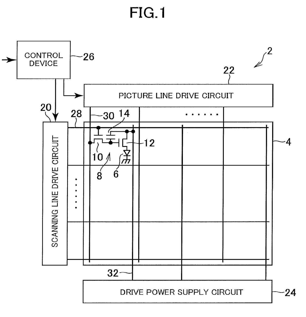
[0016]FIG. 1 is a schematic diagram showing a schematic configuration of a display device according to one embodiment of the invention using an organic EL display device as an examp...


PUM


Abstract

A method of manufacturing a display device according to an embodiment of the present invention includes: placing a component via an adhesive material on one side of a base material containing a resin; forming a hard layer on the other side of the base material at least in correspondence with an area in which the component is placed; and mounting the component on the base material by sandwiching and pressurizing the base material, the component, and the hard layer using a pair of heads. A display area including a plurality of pixels is formed on the one side of the base material.

Description

CROSS-REFERENCE TO RELATED APPLICATION[0001]The present application claims priority from Japanese Application JP2017-109995 filed on Jun. 2, 2017, the content of which is hereby incorporated by reference into this application.BACKGROUND OF THE INVENTION1. Field of the Invention[0002]One or more embodiments of the present invention relate to a display device and a method of manufacturing a display device.2. Description of the Related Art[0003]In a display device including a display area such as an organic electroluminescence (EL) display device and a liquid crystal display device, recently, development of a flexible display having a bendable display panel using a base material having flexibility has been advanced.[0004]For example, as disclosed in JP 2011-187446 A, the base material having flexibility is supported by a support substrate (e.g. glass substrate) in the manufacturing process of the display panel in view of handling ability or the like, and separated from the support subs...

Claims


Application Information

Patent Timeline
IPC IPC(8): H01L51/56H01L27/12H01L51/52G09G3/3225
CPCH01L51/56H01L27/1214H01L51/5203H01L51/524G09G3/3225G09G3/3233G09G2300/0426H10K50/841H10K71/00H10K50/805
Inventor ODAKA, KAZUHIRO
Owner JAPAN DISPLAY INC
Why Eureka
Try Eureka