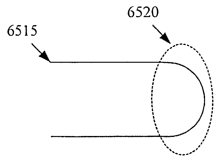
Circular vias and interconnect-line ends
a technology of interconnecting lines and vias, which is applied in the direction of cad circuit design, instrumentation, and semiconductor/solid-state device details, etc., can solve the problems of not being able to explore diagonal routing paths consistently, affecting the design of the layer, and affecting the performance of the layer
- Summary
- Abstract
- Description
- Claims
- Application Information
AI Technical Summary
Problems solved by technology
Method used
Image

Examples
Embodiment Construction
[0071]In the following description, numerous details are set forth for purpose of explanation. However, one of ordinary skill in the art will realize that the invention may be practiced without the use of these specific details. In other instances, well-known structures and devices are shown in block diagram form in order not to obscure the description of the invention with unnecessary detail.
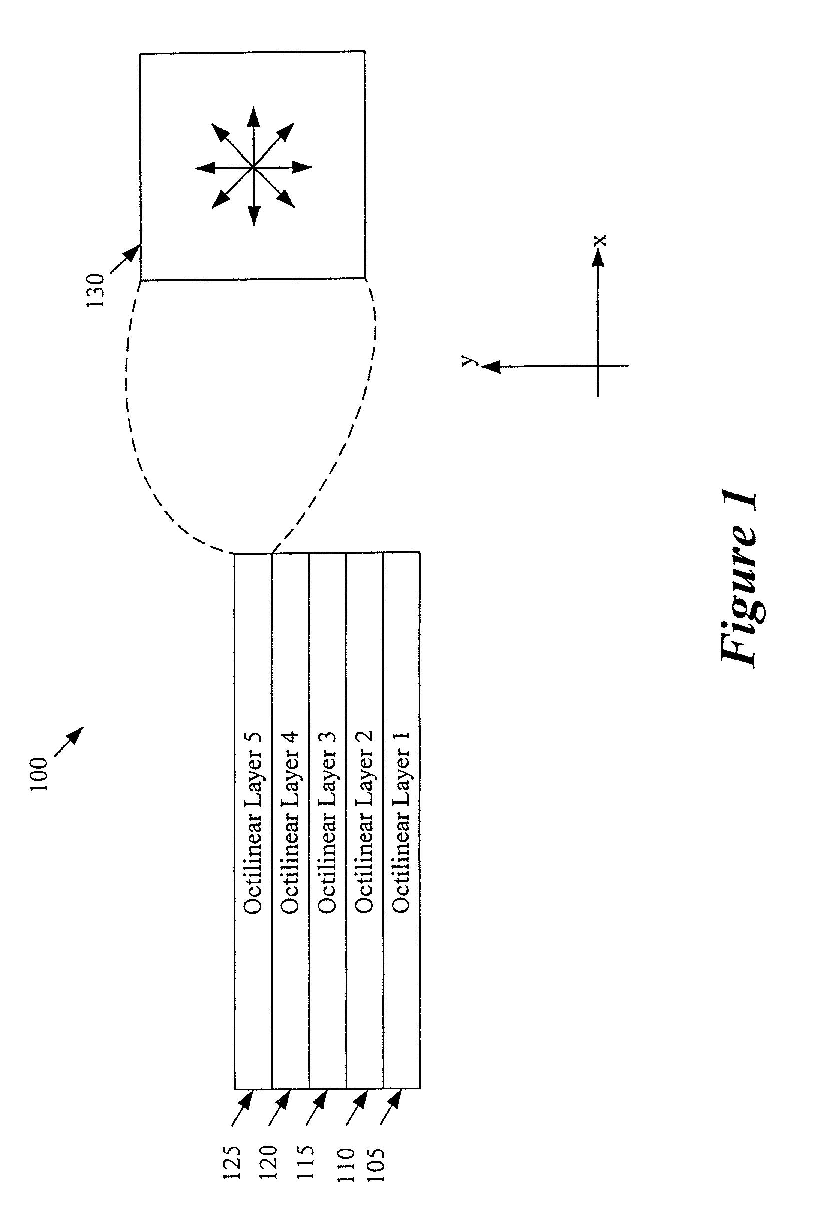
I. Non-Preferred Direction Architecture
[0072]Some embodiments of the invention utilize non-preferred-direction (“NPD”) wiring models for designing IC layouts. A NPD wiring model does not specify a single preferred routing direction for at least one of its interconnect layers. (In the discussion below, the terms interconnect layer is interchangeably used with the terms metal or wiring layer.)
[0073]A NPD wiring model has at least one NPD interconnect layer that has more than one preferred routing direction. In other words, each NPD interconnect layer has at least two routing directions that are e...
PUM
 Abstract
Description
Claims
Application Information
 - R&D Engineer
- R&D Manager
- IP Professional
- Industry Leading Data Capabilities
- Powerful AI technology
- Patent DNA Extraction
Browse by: Latest US Patents, China's latest patents, Technical Efficacy Thesaurus, Application Domain, Technology Topic.
© 2024 PatSnap. All rights reserved.Legal|Privacy policy|Modern Slavery Act Transparency Statement|Sitemap