Organic semiconductor sensor device

a sensor device and organic semiconductor technology, applied in thermoelectric devices, acquiring/reconfiguring fingerprints/palmprints, instruments, etc., can solve the problems of limited number of organic semiconductor materials that are n-type, limited the functionality of organic semiconductor devices, and limited practical applications

Inactive Publication Date: 2006-11-28
STMICROELECTRONICS INC
View PDF6 Cites 13 Cited by
  • Summary
  • Abstract
  • Description
  • Claims
  • Application Information

AI Technical Summary

Benefits of technology

[0009]In a preferred implementation, the present invention provides an organic semiconductor sensor device in which a sensor element has a capacitance that varies with the dimensions of a depletion region. The capacitance may vary in response to an object that may be on or proximate to a sensing surface of the sensor element, thereby modulating the depletion region.

Problems solved by technology

However, as observed in U.S. Pat. No. 6,252,245, only a limited number of organic semiconductor materials have been developed that are n-type.
This has restricted the functionality of organic semiconductor devices and limited their practical applications.

Method used


Image

  • Organic semiconductor sensor device
  • Organic semiconductor sensor device
  • Organic semiconductor sensor device

Examples


Embodiment Construction

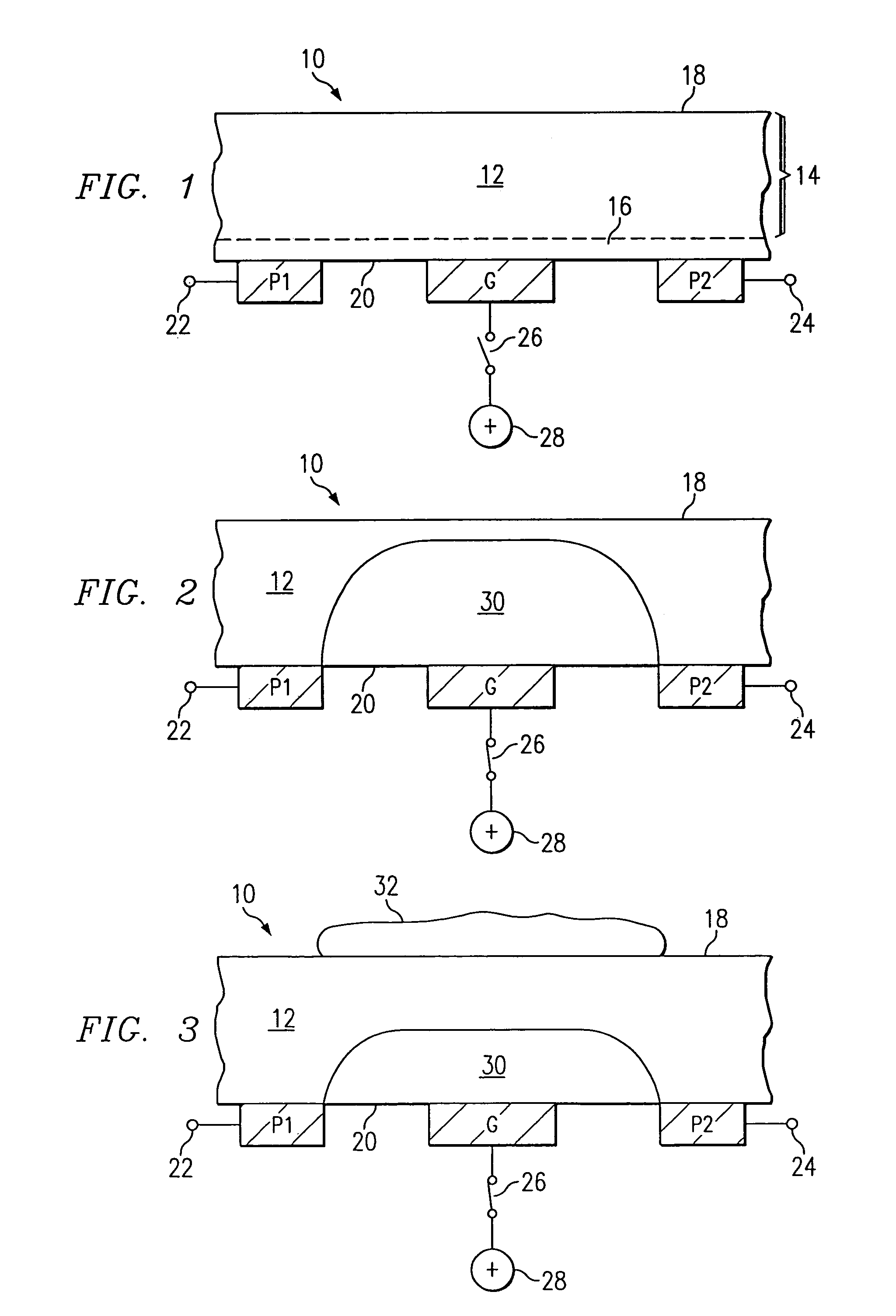
[0028]With reference to FIG. 1, a sensor element in accordance with the invention is designated generally by reference numeral 10. The sensor element 10 may have useful applications both as a single such element in a sensing device or as one of many such elements incorporated into an array forming part of a sensor device. The element 10 includes an organic semiconductor layer 12 that can comprise any suitable organic semiconductor material, such as pentacene, that can be prepared with regions of negative and / or positive mobile charges. In its simplest form, the organic semiconductor layer 12 can be chemically structured to provide a uniform distribution of positive majority mobile charge carriers when the layer 12 is in an unbiased state. The sensor element 10 can be constructed from organic semiconductor material having majority mobile charge carriers of either conductivity type. FIG. 1 shows an alternative having a non-uniform distribution of p-type conductivity material in which ...


PUM

PropertyMeasurementUnit
semiconductoraaaaaaaaaa
charge carriersaaaaaaaaaa
charge carrier mobilitiesaaaaaaaaaa

Abstract

Sensor cells are arranged in an array in an organic semiconductor layer. Row and column select circuitry addresses the cells of the array one cell at a time to determine the presence of an object, such as a fingerprint ridge or valley, contacting or proximate to a sensing surface above each cell. Control circuitry can be provided in a companion silicon chip or in a second layer of organic semiconductor material to communicate with the array and an associated system processor. The array of sensor cells can be fabricated using a flexible polymer substrate that is peeled off and disposed of after contacts have been patterned on the organic semiconductor layer. The organic semiconductor layer can be used with a superimposed reactive interface layer to detect specific chemical substances in a test medium.

Description

CROSS-REFERENCE TO RELATED APPLICATION[0001]This application is a division of application Ser. No. 10 / 254,311 filed Sep. 25, 2002 now U.S. Pat. No. 6,852,996.TECHNICAL FIELD OF THE INVENTION[0002]The present invention relates generally to devices and methods of device fabrication using organic semiconductor materials, and more particularly to sensor devices having an organic semiconductor layer that performs a sensing function.BACKGROUND OF THE INVENTION[0003]It is well known that organic polymeric materials can have compositions that produce mobile charge carriers, enabling the manufacture of organic semiconductor devices. U.S. Pat. No. 4,222,903 discloses a p-type conductivity polyacetylene film that can be doped with acceptor dopants to selectively increase its p-type electrical conductivity. A semiconductor material is known as “p-type” conductivity when its majority mobile charge carriers are positive charge carriers called “holes.” A semiconductor material is known as “n-type”...

Claims


Application Information

Patent Timeline
Patent Type & Authority Patents(United States)
IPC IPC(8): H01L27/28G01B7/28G01N27/414G01N33/487G06K9/00G06T1/00H01L51/05
CPCG01L1/146G01L1/148G06K9/0002H01L27/307G01N27/4145G01N27/4148H01L51/0508G06V40/1306H10K39/32H10K10/46
Inventor THOMAS, DANIELLE A.DEBEURRE, BRUNO J.THOMA, PETER J.
Owner STMICROELECTRONICS INC
Why Eureka
Try Eureka