Semiconductor substrate, semiconductor device, and method of manufacturing the same
a semiconductor and substrate technology, applied in the direction of semiconductor devices, electrical devices, transistors, etc., can solve the problems of high crystallinity, low manufacturing efficiency, and increased leakage current, and achieve the effect of efficient straining a semiconductor layer or semiconductor region
- Summary
- Abstract
- Description
- Claims
- Application Information
AI Technical Summary
Benefits of technology
Problems solved by technology
Method used
Image

Examples
first embodiment
(First Embodiment)
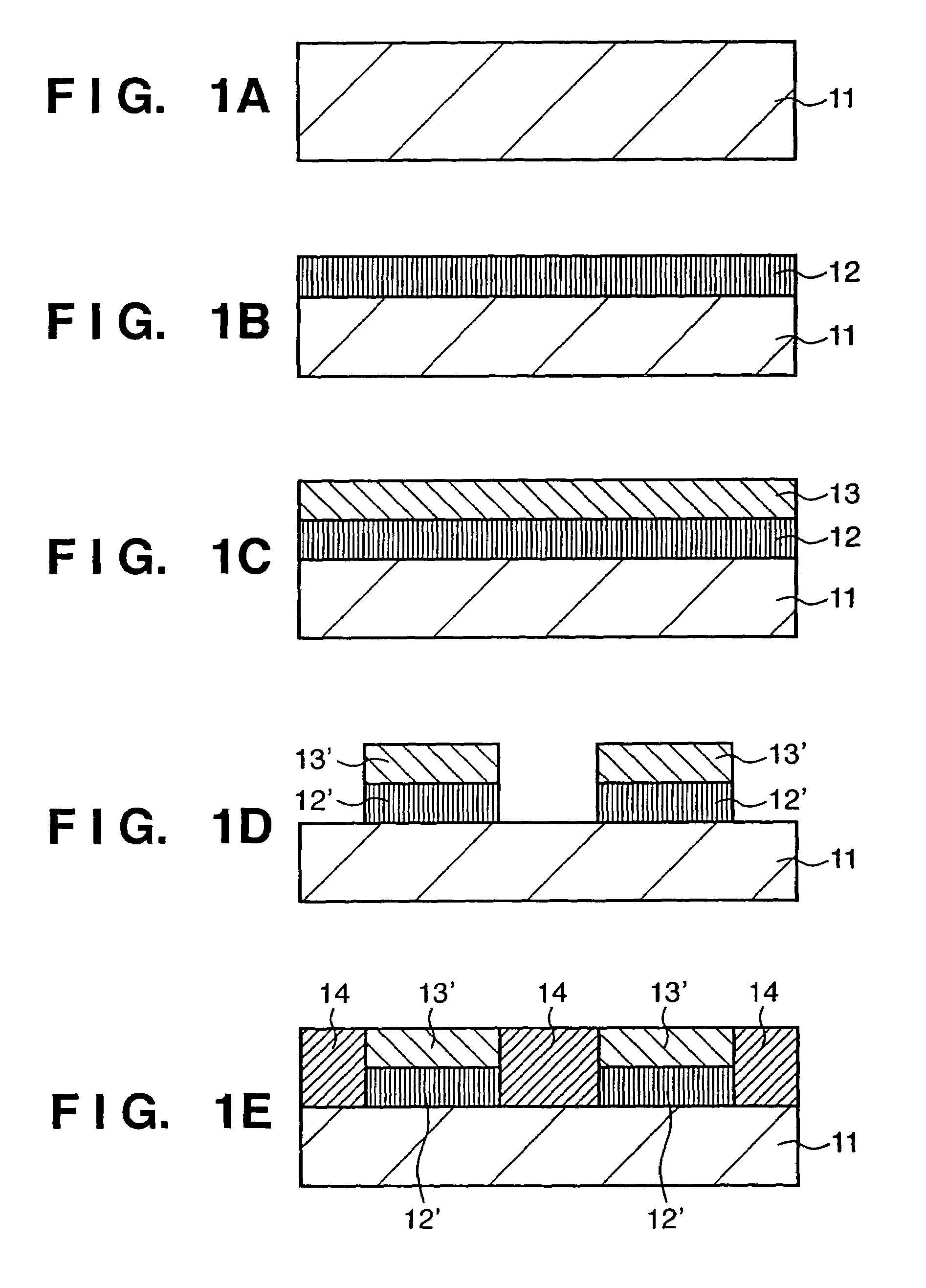
[0033]FIGS. 1A to 1E are sectional views for explaining a substrate manufacturing method according to the preferred first embodiment of the present invention.
[0034]In the step shown in FIG. 1A, a substrate 11 is prepared. As the substrate 11, for example, silicon is preferable. However, any other material may be employed.
[0035]In the step shown in FIG. 1B, a porous layer 12 is formed on the surface of the substrate 11. The Young's modulus of the porous layer 12 is lower than that of a semiconductor layer 13 to be formed in the step shown in FIG. 1C. As the material of the porous layer 12, porous silicon prepared by porosifying silicon is preferably employed. A porous silicon layer can be formed by anodizing the surface of the silicon substrate. Anodizing can be executed by arranging an anode and a cathode in an electrolytic solution containing hydrofluoric acid, placing the substrate between the electrodes, and supplying a current between the electrodes.
[0036]The p...
second embodiment
(Second Embodiment)
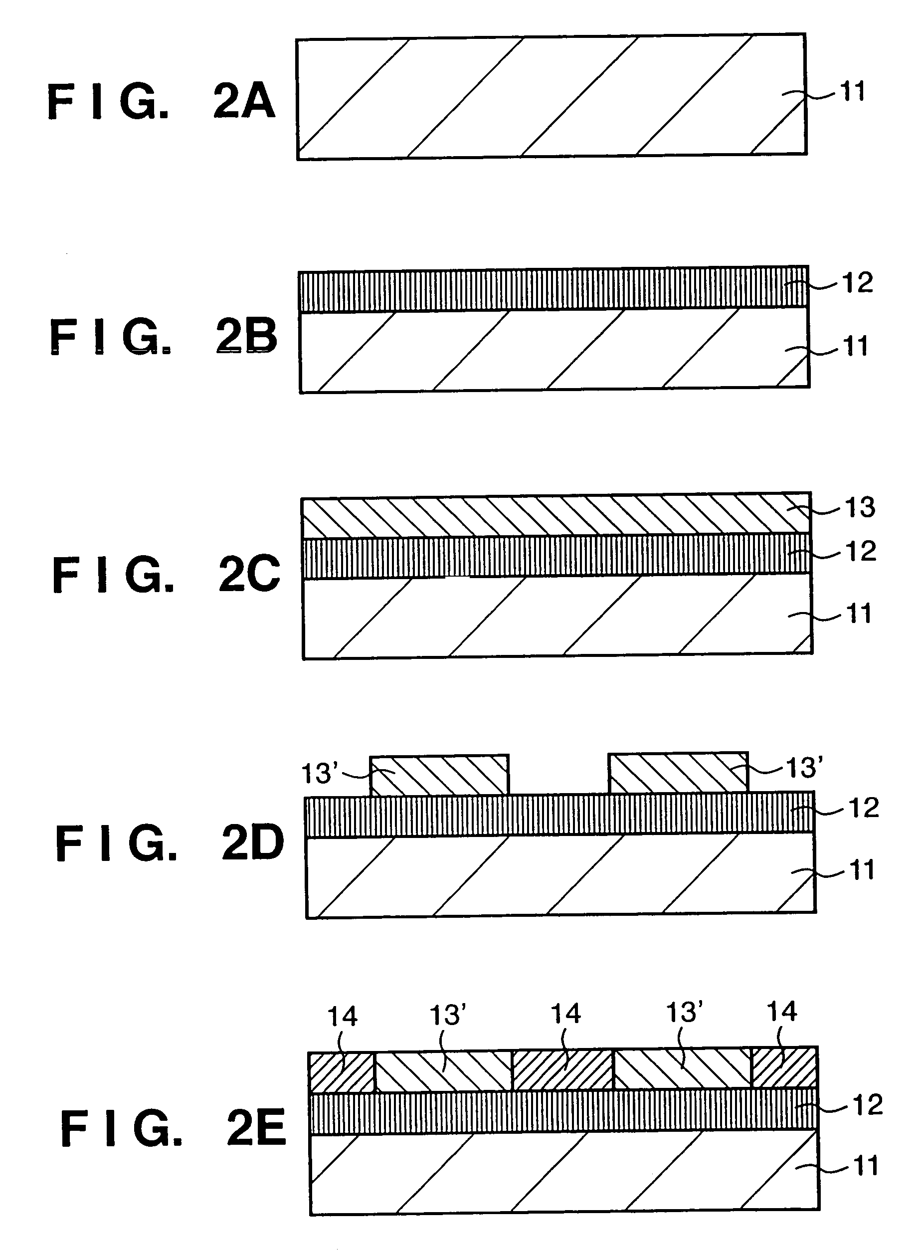
[0048]A substrate manufacturing method according to the preferred second embodiment of the present invention will be described next. In the substrate manufacturing method according to this embodiment, some steps in the substrate manufacturing method according to the first embodiment are changed. FIGS. 2A to 2E are sectional views for explaining the substrate manufacturing method according to the second embodiment. The steps shown in FIGS. 2A to 2C are the same as those shown in FIGS. 1A to 1C.
[0049]In the step shown in FIG. 2D, a semiconductor layer 13 is etched to form opening portions. In the step shown in FIG. 2E, a strain inducing region 14 is formed on a porous layer 12 exposed to each opening portion. With the above structure, a semiconductor layer 13′ formed on the porous layer 12 can efficiently be strained.
third embodiment
(Third Embodiment)
[0050]A substrate manufacturing method according to the preferred third embodiment of the present invention will be described next. In the substrate manufacturing method according to this embodiment, some steps in the substrate manufacturing method according to the first embodiment are changed. FIGS. 3A to 3E are sectional views for explaining the substrate manufacturing method according to the third embodiment. The steps shown in FIGS. 3A and 3C are the same as those shown in FIGS. 1A and 1C.
[0051]In the step shown in FIG. 3B, porous layers are partially formed in a substrate 11. When anodizing is employed as a method of forming the porous layer, for example, a protective film (e.g., a nitride film or HF-resistant mask) which protects the substrate from the chemical solution (e.g., hydrofluoric acid) used in anodizing is formed on the substrate 11. After that, the substrate 11 is anodized to form partial porous layers 12′ shown in FIG. 3B. In the step shown in FIG...
PUM
 Abstract
Description
Claims
Application Information
 - Generate Ideas
- Intellectual Property
- Life Sciences
- Materials
- Tech Scout
- Unparalleled Data Quality
- Higher Quality Content
- 60% Fewer Hallucinations
Browse by: Latest US Patents, China's latest patents, Technical Efficacy Thesaurus, Application Domain, Technology Topic, Popular Technical Reports.
© 2025 PatSnap. All rights reserved.Legal|Privacy policy|Modern Slavery Act Transparency Statement|Sitemap|About US| Contact US: help@patsnap.com