Semiconductor device and method for manufacturing thereof

Inactive Publication Date: 2007-02-27
KK TOSHIBA
View PDF5 Cites 1 Cited by
  • Summary
  • Abstract
  • Description
  • Claims
  • Application Information

AI Technical Summary

Problems solved by technology

However, in the light of the current circumstances, the polarization amount obtained by the capacitor having a conventional structure in which a PZT thin film is sandwiched between SRO electrodes, is still not enough and there is an increasing demand for a further improvement in the polarization amount.

Method used


Image

  • Semiconductor device and method for manufacturing thereof
  • Semiconductor device and method for manufacturing thereof
  • Semiconductor device and method for manufacturing thereof

Examples


Embodiment Construction

[0020]An embodiment of the present invention will now be described with reference to accompanying drawings.

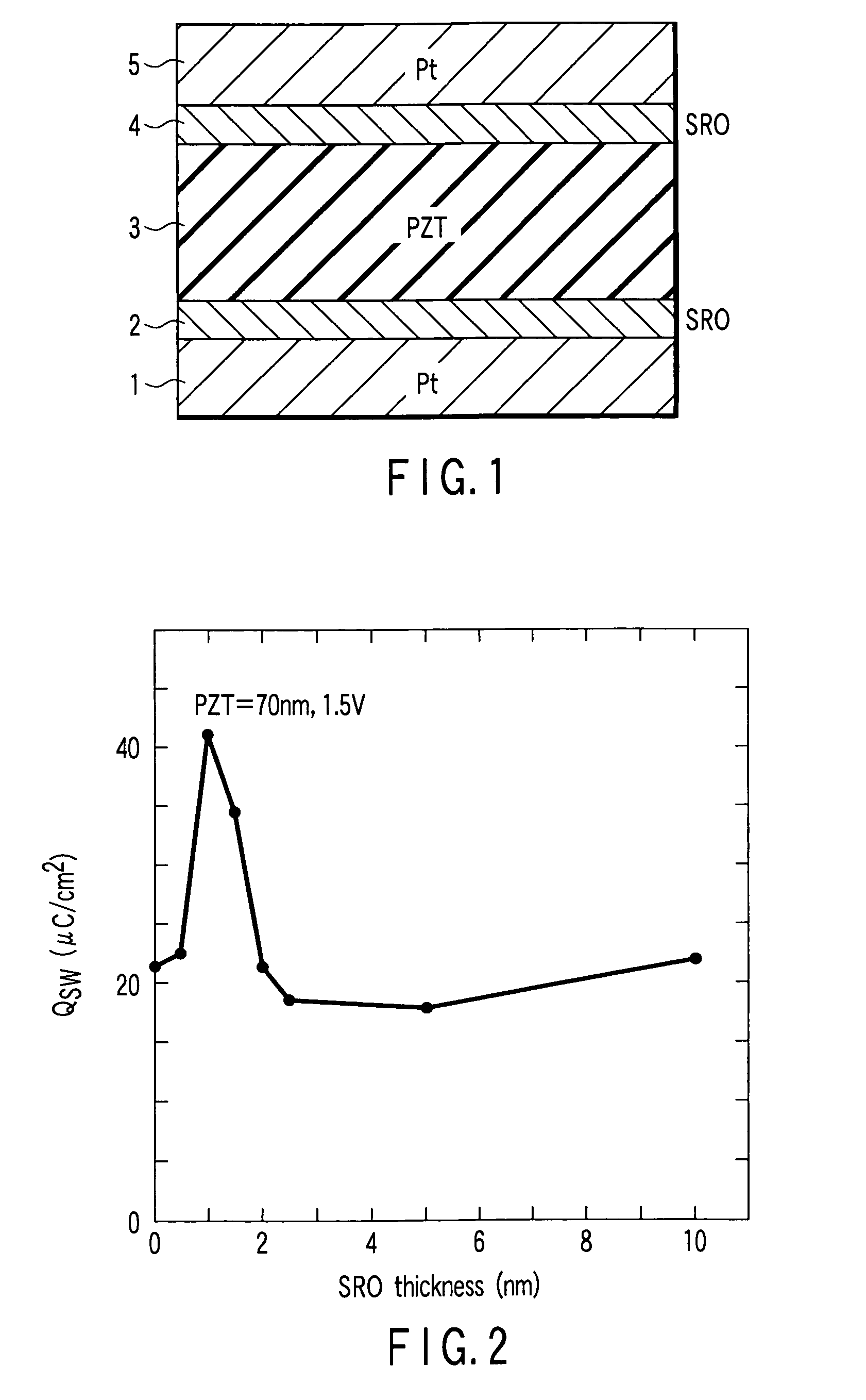
[0021]The inventor of the present invention discovered that when a PZT film is formed on a conventional lower SRO electrode, PZT is randomly oriented. The inventor further found that the cause that a sufficient polarization amount cannot be obtained in the conventional capacitor resides in the random orientation of PZT. Under the circumstances, the invention carried out intensive studies focusing on the orientation of PZT and has found that PZT can be made to have a desired orientation, more specifically, a priority orientation of (111) by setting the thickness of the lower SRO film to 2 nm or less. Based on this finding, the present invention has been achieved.

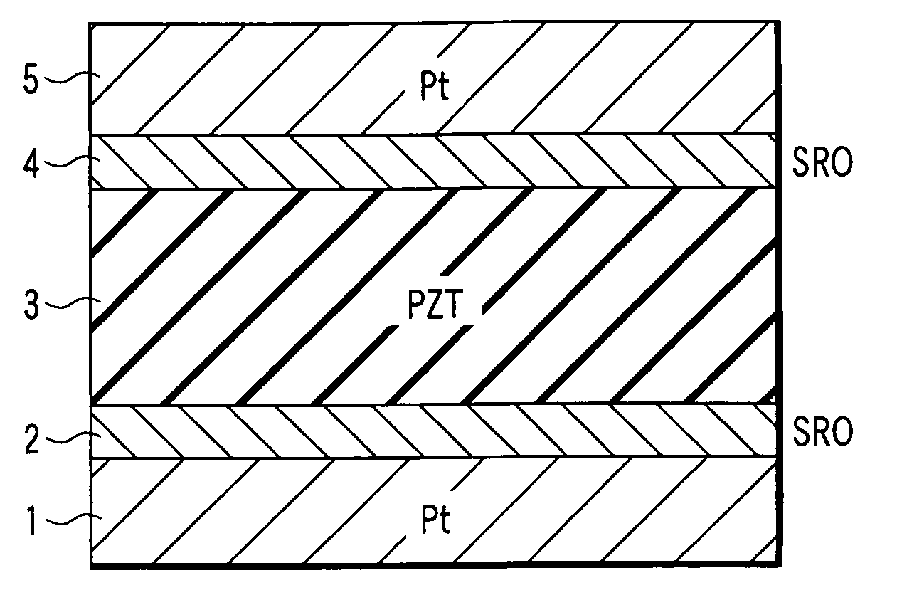
[0022]FIG. 1 is a schematic diagram showing the layer structure of a semiconductor device according to an embodiment of the present invention. The semiconductor device shown in this figure is a capacitor that employs ele...


PUM


Abstract

Disclosed in a semiconductor device comprising a semiconductor substrate, and a ferroelectric layer provided above the semiconductor substrate and sandwiched between a lower electrode and an upper electrode, the lower electrode comprising a strontium ruthenate film having a thickness of 2 nm or less.

Description

CROSS-REFERENCE TO RELATED APPLICATIONS[0001]This application is based upon and claims the benefit of priority from prior Japanese Patent Application No. 2004-112466, filed Apr. 6, 2004, the entire contents of which are incorporated herein by reference.BACKGROUND OF THE INVENTION[0002]1. Field of the Invention[0003]The present invention relates to a semiconductor device and a method of manufacturing the device.[0004]2. Description of the Related Art[0005]A widely popular capacitor of a ferroelectric memory employs the structure that a lead zirconate titanate (Pb(ZrxTi1-x)O3, to be called PZT hereinafter) thin film is sandwiched between a pair of electrodes. When a voltage is applied to this structure, the PZT is polarized. This polarization is not canceled if the power is turned off, and therefore the polarization can serve as a nonvolatile memory. As the polarization amount of the ferroelectric layer becomes larger, the signal amount is increased, and a device with a higher perform...

Claims


Application Information

Patent Timeline
Patent Type & Authority Patents(United States)
IPC IPC(8): H01L29/76H01L21/3205H01L21/02H01L21/8246H01L23/52H01L27/105
CPCH01L28/55H01L28/75H01L28/65
Inventor NAKAZAWA, KEISUKE
Owner KK TOSHIBA
Why Eureka
Try Eureka