Post-ESL porogen burn-out for copper ELK integration

a technology of copper elk and porogen, applied in the field of low-k dielectric layer formation method, can solve the problems of low power dissipation, high speed performance of integrated circuit, and new problems caused by the integration of porous dielectrics into conventional device fabrication schemes, so as to avoid dielectric shrinkage

Inactive Publication Date: 2007-05-15
TAIWAN SEMICON MFG CO LTD
View PDF25 Cites 23 Cited by
  • Summary
  • Abstract
  • Description
  • Claims
  • Application Information

AI Technical Summary

Benefits of technology

[0008]A preferred embodiment comprises the steps of forming a porogen-containing, low-k dielectric layer in the damascene process. In preferred embodiments, pore generation by porogen e-beam curing occurs after the steps of planarizing the damascene copper conductor and depositing a semipermeable cap layer. Preferred embodiments advantageously avoid dielectric shrinkage caused by reaction of the porogen. Preferred embodiments also avoid a pore sealing manufacturing step before building the damascene structure.

Problems solved by technology

Such lower capacitance results in higher speed performance of the integrated circuit and also in lower power dissipation.
Integration of porous dielectrics into conventional device fabrication schemes has created new problems.
Moreover, the introduction of nanopores drastically deteriorates the mechanical properties of the film thereby limiting the yield of chemical mechanical polishing in copper-ELK (extreme low-k dielectric) process integration.

Method used


Image

  • Post-ESL porogen burn-out for copper ELK integration
  • Post-ESL porogen burn-out for copper ELK integration
  • Post-ESL porogen burn-out for copper ELK integration

Examples


Embodiment Construction

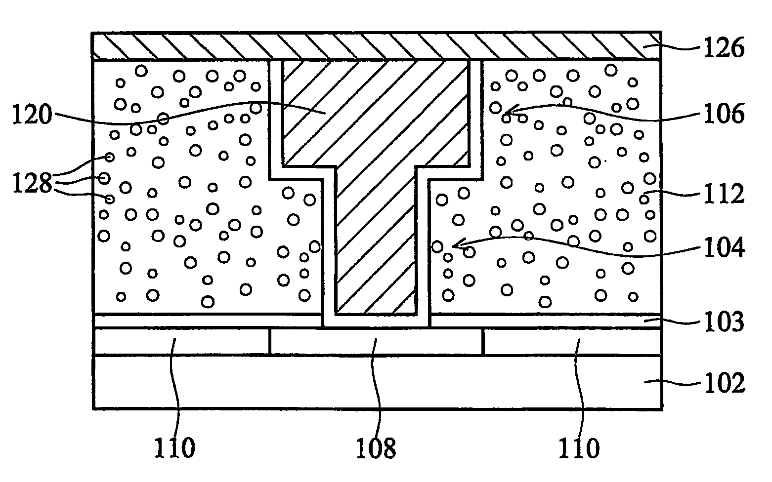
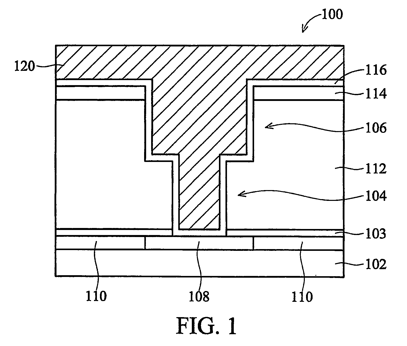
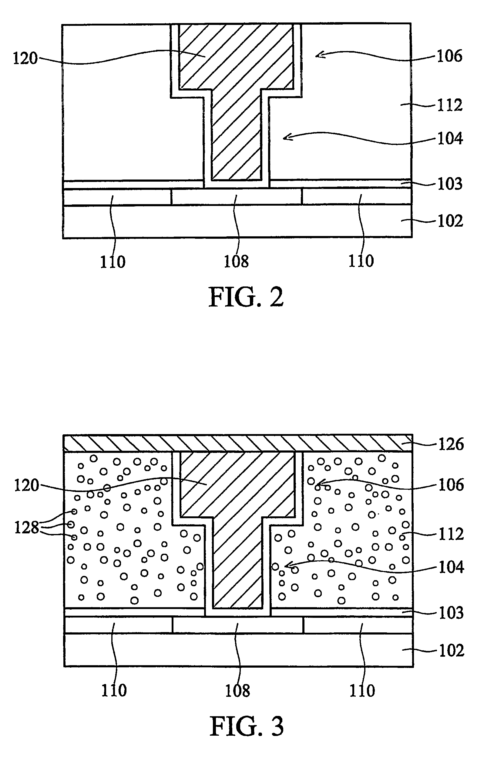
[0016]The operation and fabrication of the presently preferred embodiments are discussed in detail below. However, the embodiments and examples described herein are not the only applications or uses contemplated for the invention. The specific embodiments discussed are merely illustrative of specific ways to make and use the invention, and do not limit the scope of the invention or the appended claims.

[0017]This invention relates generally to semiconductor device fabrication and more specifically to porous, low-k dielectric formation by degradation of a porogen. This integration scheme uses a spun-on, dielectric material in a non-porous state that withstands the processing steps associated with advanced interconnect fabrication. Device fabrication steps such as etching, lithography, metal deposition, and CMP can be accomplished on a non-porous dielectric. The porogen degradation is performed after interlevel integration.

[0018]The present invention will now be described with respect ...


PUM

PropertyMeasurementUnit
pressureaaaaaaaaaa
temperatureaaaaaaaaaa
dielectric constantaaaaaaaaaa

Abstract

A method of manufacturing a semiconductor device having a porous, low-k dielectric layer is provided. A preferred embodiment comprises the steps of forming a porogen-containing, low-k dielectric layer, in the damascene process. In preferred embodiments, pore generation, by e-beam porogen degradation, occurs after the steps of CMP planarizing the damascene copper conductor and depositing a semipermeable cap layer. In alternative embodiments, the cap layer consists essentially of silicon carbide, silicon nitride, Co, W, Al, Ta, Ti, Ni, Ru, and combinations thereof. The semipermeable cap layer is preferably deposited under PECVD conditions such that the cap layer is sufficiently permeable to enable removal of porogen degradation by-products. Preferred embodiments further include an in-situ N2 / NH3 treatment before depositing the semipermeable cap layer.

Description

TECHNICAL FIELD[0001]This invention relates generally to semiconductor device fabrication and more particularly to a method for forming a porous, low-k dielectric layer.BACKGROUND[0002]An important objective in the advancement of integrated circuit (IC) technology is the scaling-down of IC dimensions. Such scaling-down of IC dimensions reduces area capacitance and is critical to obtaining higher speed performance of integrated circuits. Moreover, reducing the area of an IC die leads to higher yield in IC fabrication. Such advantages are a driving force to constantly scale down IC dimensions.[0003]As the density of integrated circuit structures continually increases, the distance between the interconnect structures decreases. As the distance between the interconnect structures decreases, a dielectric material with a low dielectric constant (i.e., a low-k dielectric material) is desired for the insulating layer. The insulating layer being comprised of the dielectric material with a lo...

Claims


Application Information

Patent Timeline
Patent Type & Authority Patents(United States)
IPC IPC(8): H01L21/4763
CPCH01L21/02126H01L21/02203H01L21/02282H01L21/02304H01L21/0234H01L21/02362H01L21/3122H01L21/3148H01L21/31695H01L21/76807H01L21/7682H01L21/76834H01L21/76843H01L21/76846H01L21/7685H01L2221/1047
Inventor LU, YUNG-CHENGCHEN, YING-TSUNGWU, ZHEN-CHENGCHEN, PI-TSUNG
Owner TAIWAN SEMICON MFG CO LTD
Why Eureka
Try Eureka