

Estimation circuit for time-interleaved ADC and method thereof
a time-interleaved adc and estimation circuit technology, applied in the field of correlation circuits for adc, can solve problems such as timing errors, gain errors, offset errors, and errors, and achieve the effect of reducing the efficiency of time-interleaved ad
- Summary
- Abstract
- Description
- Claims
- Application Information
AI Technical Summary
Problems solved by technology
Method used
Image

Examples
first embodiment
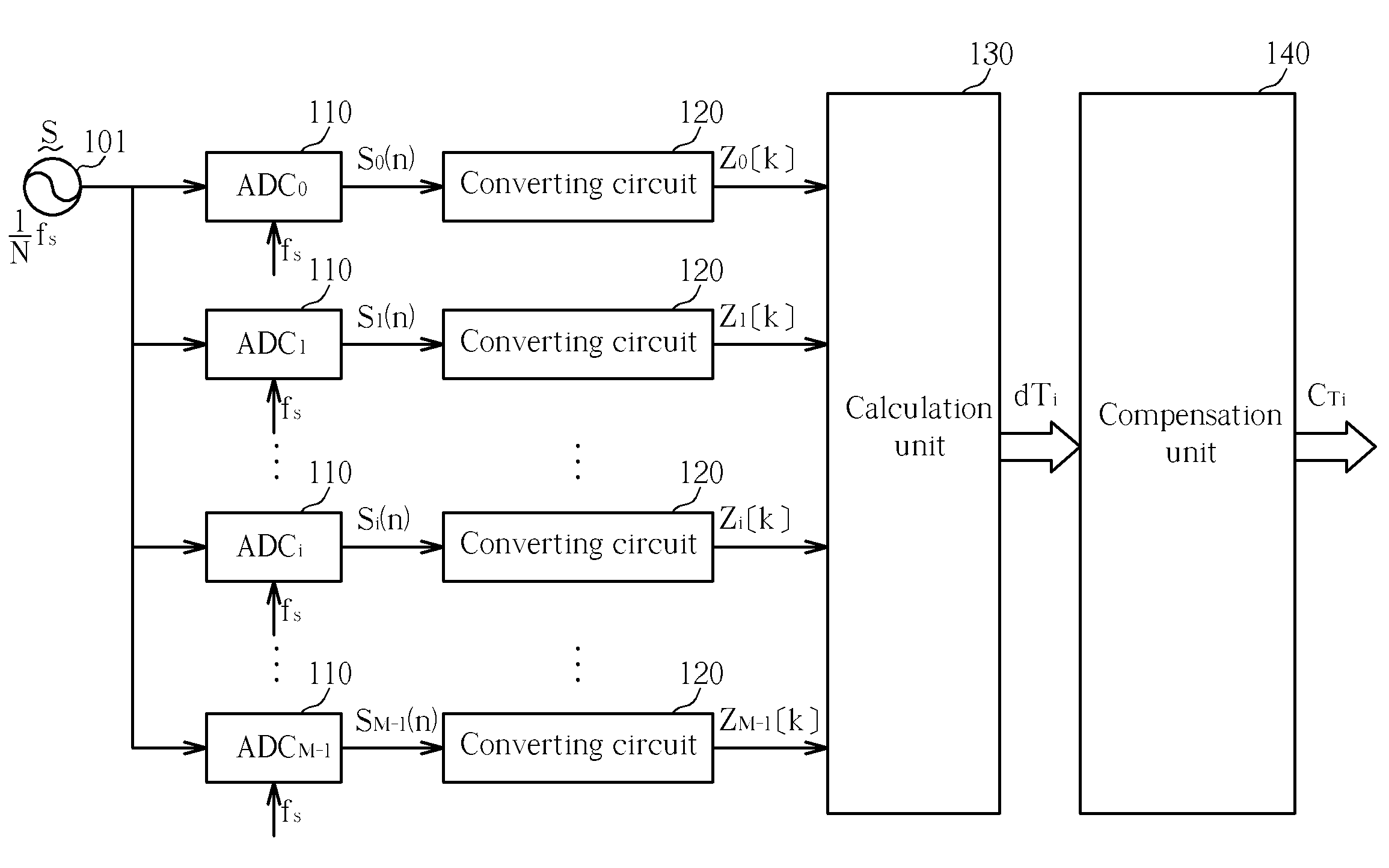
[0020]FIG. 1 shows a time-interleaved ADC according to the present invention. It is assumed that M ADC 110 (ADC0, ADC1, . . . , ADCM−1) are included, and each has a sampling frequency of fs. Each ADC 110 receives an analog sine wave S from a signal generator 101. The sine wave S has a frequency of fs / N, N being an integer, i.e., the sampling frequency of each ADC 110 is N multiple of the frequency of the sine wave S. Theoretically, the sampling timings of M ADC 110 should distribute uniformly within one period T=1 / fs, i.e., the sampling timing difference between two adjacent ADCs is T / M. Moreover, practically, for the (i+1)th ADCi, the relationship between the input signal xi and the output yi is expressed as follows (quantization error is neglected):
yi=(1+ai)xi+bi
[0021]wherein, ai is the gain error of the (i+1)th ADCi, and bi is the offset error. The correction method disclosed in this invention observes the output signals of each ADC in digital domain, and then filters out unneces...
second embodiment
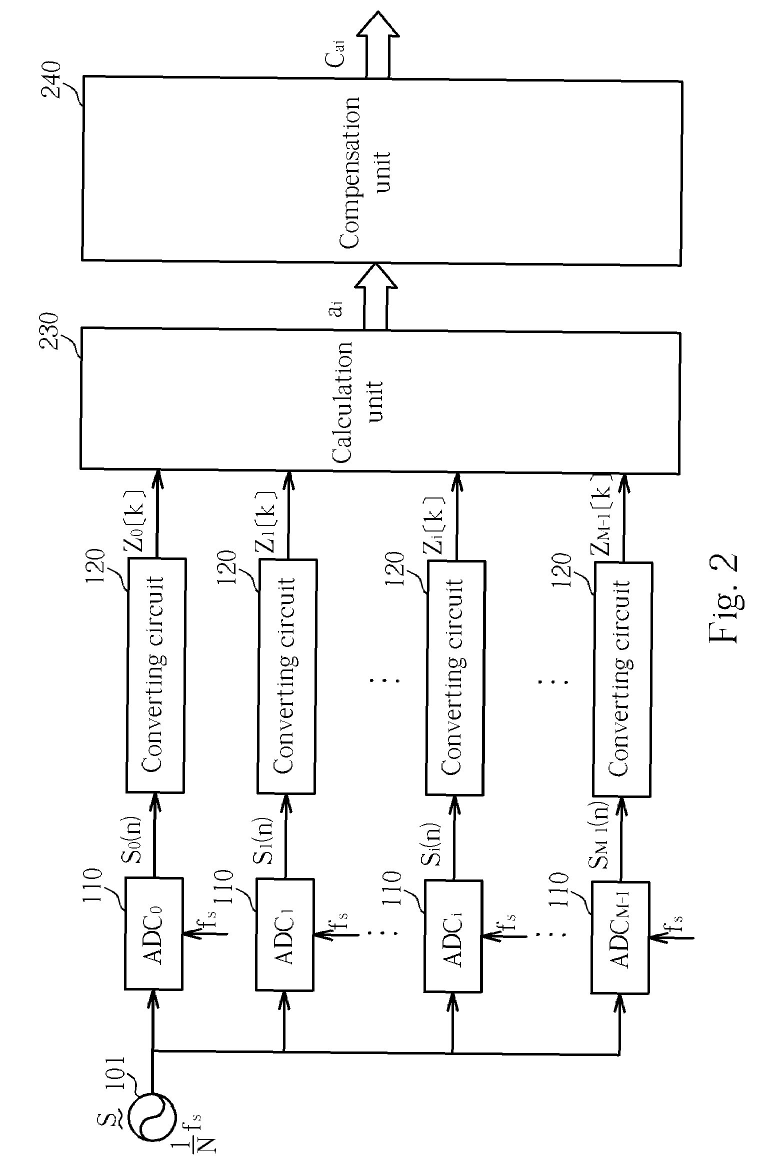
[0034]FIG. 2 shows a correction circuit for a time-interleaved ADC according to the present invention. The calculation unit 230 collects all complex numbers (Z0[k],Z1[k], . . . ,ZM−1[k]) generated by the converting circuit 120 and thereby calculates the modulus (|Z0|, |1|, . . . , |ZM−1|) of each complex number. Each modulus has information about the gain error of its corresponding ADC 110. The calculation unit 230 further calculates gain errors of each ADC according to the modulus. If the first ADC0 establishes the criteria, the gain error ai of the (i+1)th ADCi can be expressed as:
[0035]ai=Zi-Z0Z0Eq.(6)
[0036]As a result, the calculation unit 230 will output a number of M−1 gain errors (a1,a2, . . . ,aM−1) to the compensation unit 240. The compensation unit 240 generates a plurality of compensation signals Cai according to the M−1 gain errors to respectively compensate ADC1˜ADCM−1. Please note that in these two embodiments mentioned above, the criteria can be established utilizing...
third embodiment
[0037]FIG. 3 shows a correction circuit for a time-interleaved ADC according to the present invention. The third embodiment is similar to the first and the second embodiments. After sampling the analog sine wave S, each ADC 110 generates a set of sampled data. In this embodiment, each ADC 110 is coupled to a calculation unit 310. The calculation unit 310 calculates the average value of every set of sampled data. That is, the calculation unit 310 calculates each set of sample data (S0(n), S1(n), . . . ,SM−1(n)) to generate the corresponding average values (b0, b1, . . . ,bM−1). The compensation unit 320 receives these average values and takes a certain ADC, e.g., ADC0, as the criteria, the offset error Bi of the (i+1)th ADCi can be expressed as:
Bi=bi−b0 Eq. (7)
[0038]As a result, the compensation unit 320 will output a plurality of compensation signals CBi according to the M−1 offset errors to correct offsets of ADC1˜ADCM−1.
[0039]The detailed circuitry of the converting circuit 120 s...
PUM
 Abstract
Description
Claims
Application Information