Wide-band high-gain limiting amplifier with parallel resistor-transistor source loads

a high-gain, amplifier technology, applied in differential amplifiers, amplifiers with semiconductor devices/discharge tubes, amplifier details, etc., can solve problems such as variable delay and high-frequency components, and achieve the effect of reducing distortion

Inactive Publication Date: 2007-09-04
DIODES INC
View PDF20 Cites 23 Cited by
  • Summary
  • Abstract
  • Description
  • Claims
  • Application Information

AI Technical Summary

Problems solved by technology

Variable delay and high-frequency components add to the distortion.
Signal pulses may be spread out and interfere with other pulses.

Method used


Image

  • Wide-band high-gain limiting amplifier with parallel resistor-transistor source loads
  • Wide-band high-gain limiting amplifier with parallel resistor-transistor source loads
  • Wide-band high-gain limiting amplifier with parallel resistor-transistor source loads

Examples


Embodiment Construction

[0012]The present invention relates to an improvement in amplifier circuits. The following description is presented to enable one of ordinary skill in the art to make and use the invention as provided in the context of a particular application and its requirements. Various modifications to the preferred embodiment will be apparent to those with skill in the art, and the general principles defined herein may be applied to other embodiments. Therefore, the present invention is not intended to be limited to the particular embodiments shown and described, but is to be accorded the widest scope consistent with the principles and novel features herein disclosed.

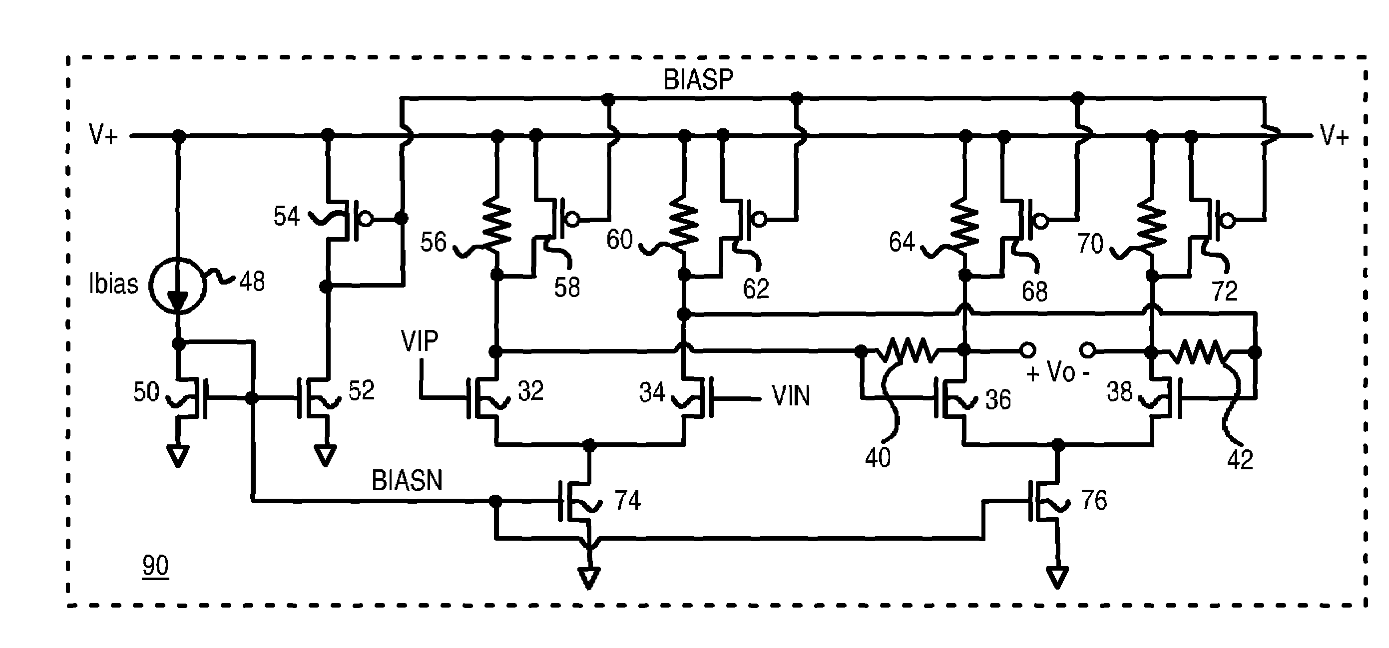
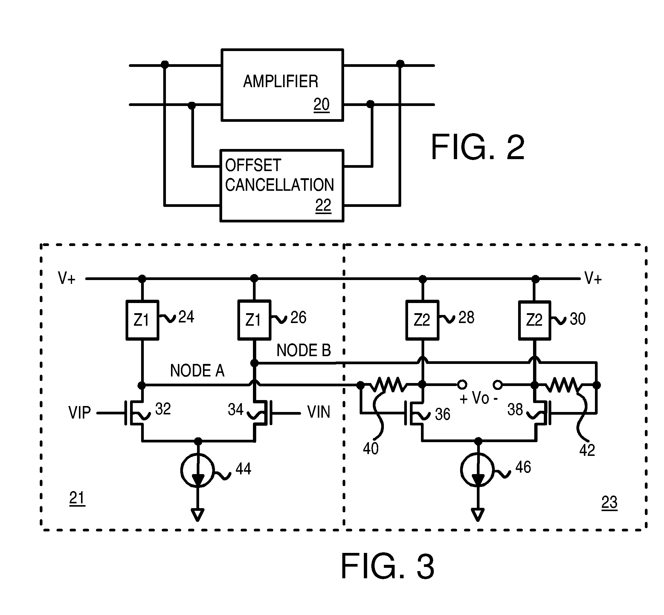
[0013]FIG. 2 shows a block diagram of an amplifier with offset cancellation. Amplifier 20 and offset cancellation 22 may be used as limiting amplifier 12 (FIG. 1) of a signal repeater, or in other applications such as data communication receivers. Offset cancellation 22 prevents the D.C. offset or bias from saturating amplifier 20....


PUM


Abstract

An amplifier has a wide bandwidth and a high gain by using parallel loads. Each load has a load resistor and a load p-channel transistor in parallel. The drain voltages of differential n-channel transistors can be set by the load resistors, while switching current is provided by the load p-channel transistors. The parallel load provides a high impedance to the drain nodes yet still provides driving current. A transconductance stage with a pair of differential transistors and two parallel loads drives a shunt-shunt-feedback stage that has another pair of differential transistors and two more parallel loads. Shunt resistors between the gate and drain of the differential transistors in the shunt-shunt-feedback stage provide shunt feedback and low impedance. Several pairs of transconductance and shunt-shunt-feedback stages can be cascaded together. The cascaded amplifier may be used as a signal repeater.

Description

FIELD OF THE INVENTION[0001]This invention relates to amplifier circuits, and more particularly to complementary metal-oxide-semiconductor (CMOS) amplifier circuits with parallel loads.BACKGROUND OF THE INVENTION[0002]High-speed signals that are transmitted through a medium such as a cable or line on a printed-circuit board (PCB) are attenuated and distorted by the medium. Variable delay and high-frequency components add to the distortion. Signal pulses may be spread out and interfere with other pulses. The length of the medium is limited by such attenuation and distortion.[0003]Signal repeaters can be added in the middle of the medium to increase the distance that signals can be transmitted. FIG. 1 shows a signal repeater that can be inserted into a medium. Equalizer 10 receives inputs from one segment of the medium. Equalizer 10 recovers the signal from the input medium, and drives a recovered signal to limiting amplifier 12. The signal is amplified and limited in voltage or signa...

Claims


Application Information

Patent Timeline
Patent Type & Authority Patents(United States)
IPC IPC(8): H03F3/45
CPCH03F1/483H03F1/486H03F3/45183H03F3/45475H03F3/45748H03F3/45973H03F2200/36H03F2200/405H03F2203/45212H03F2203/45244H03F2203/45288H03F2203/45528H03F2203/45588H03F2203/45652H03F2203/45681H03F2203/45702
Inventor LIU, WING FAATZHANG, MICHAEL Y.
Owner DIODES INC
Why Eureka
Try Eureka