Modified via bottom structure for reliability enhancement
What is AI technical title?
AI technical title is built by Patsnap AI team. It summarizes the technical point description of the patent document.
a technology of reliability enhancement and bottom structure, applied in the field of modified via bottom structure for reliability enhancement, backend of the line (beol) interconnection, can solve the problem of difficult to obtain a good mechanical contact at normal chip operation temperature, and achieve good mechanical contact
Inactive Publication Date: 2007-10-16
GLOBALFOUNDRIES INC
View PDF18 Cites 22 Cited by
Summary
Abstract
Description
Claims
Application Information
AI Technical Summary
This helps you quickly interpret patents by identifying the three key elements:
Problems solved by technology
Method used
Benefits of technology
Problems solved by technology
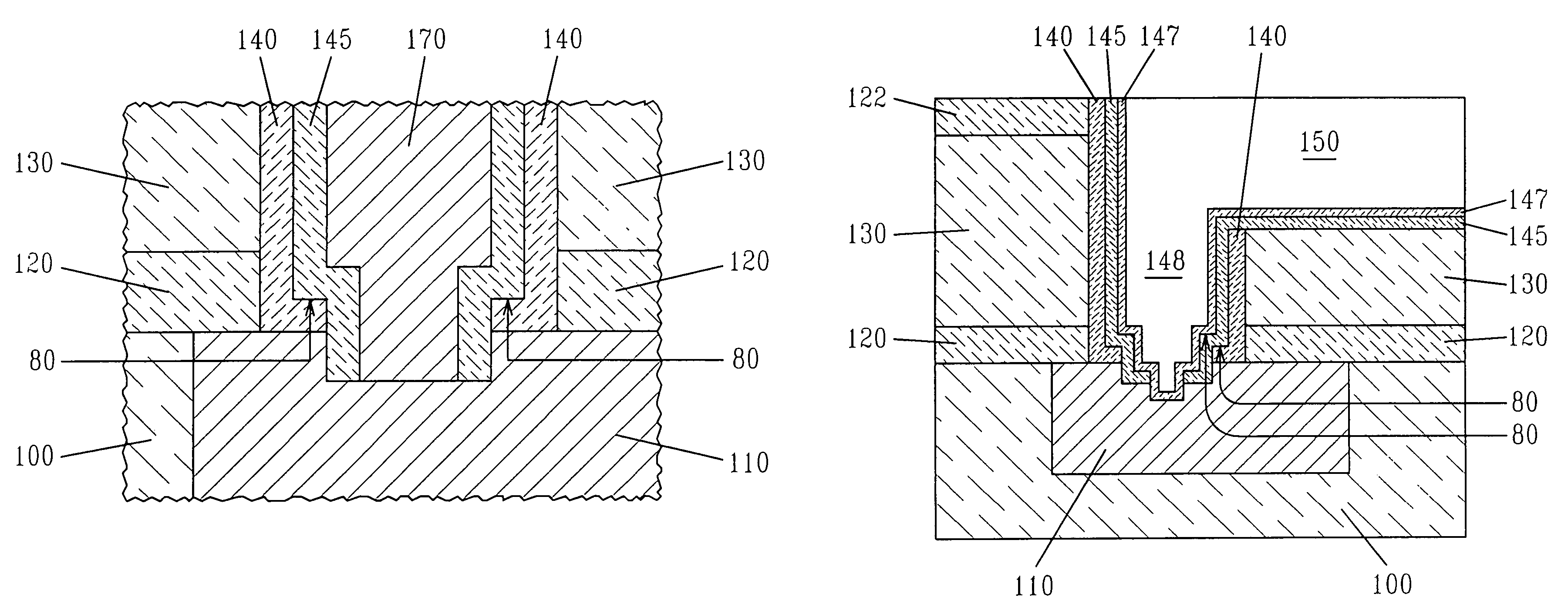
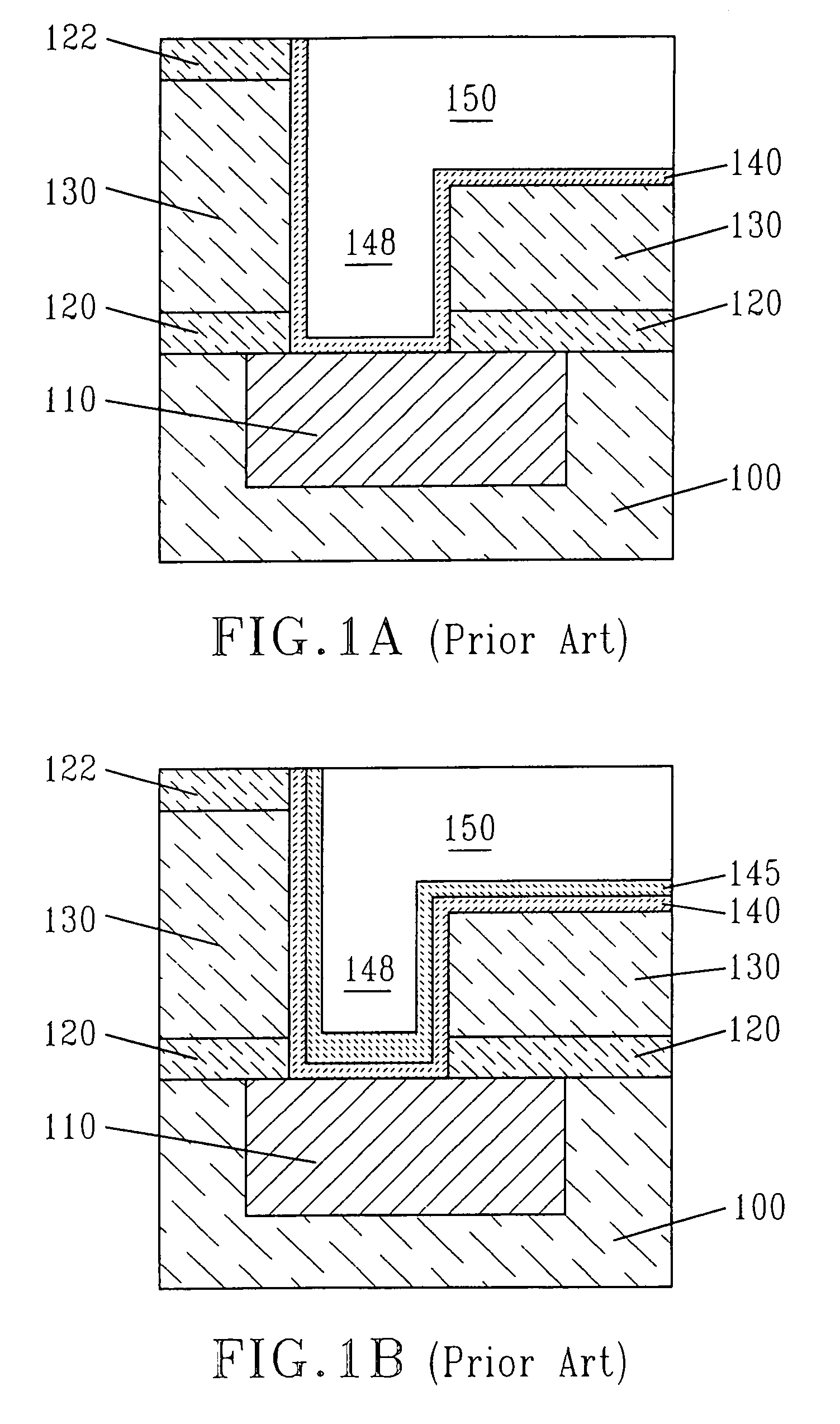
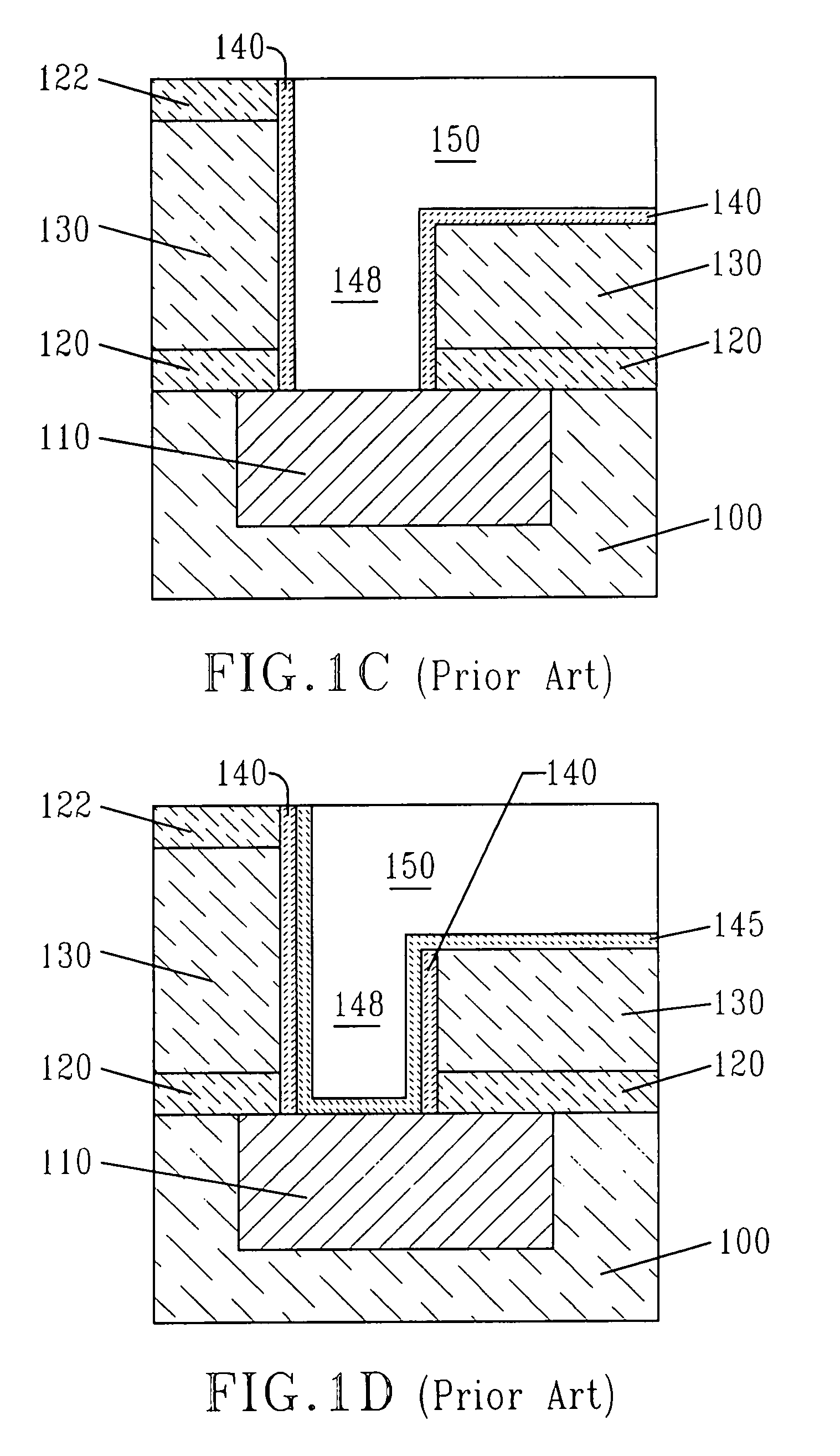
One major problem with the prior art interconnect structures shown in FIGS. 1A-1D is that it is difficult to obtain a good mechanical contact at normal chip operation temperatures.
Additionally, the prior art interconnect structures oftentimes exhibit an open circuit or high resistance joint during reliability testing.
Method used
Image
Click on the blue label to locate the original text in one second.
Reading with bidirectional positioning of images and text.
Examples
Embodiment Construction
[0030]The present invention, which provides an interconnect structure having a modified via bottom structure for reliability enhancement as well as a method of fabricating the same, will now be described in greater detail by referring to FIGS. 2-10. It is noted that FIGS. 2-10 are provided for illustrative purposes and thus they are not drawn to scale.
[0031]Reference is first made to the partial interconnect structure shown in FIG. 2 which includes a first (or lower) dielectric layer 100 having a conductive interconnect 110 embedded within a surface of the first dielectric layer 100 and an optional patterned cap 120 having an opening that exposes a surface of the conductive interconnect 110 located on the first dielectric layer 100. The partial interconnect structure shown in FIG. 2 also includes a second dielectric layer 130 that has an optional patterned hard mask 122 located on a surface of the second dielectric layer 130. The second dielectric layer 130 has at least one aperture...
PUM
Abstract
The present invention provides an interconnect structure that can be made in the BEOL which exhibits good mechanical contact during normal chip operations and does not fail during various reliability tests as compared with the conventional interconnect structures described above. The inventive interconnect structure has a kinked interface at the bottom of a via that is located within an interlayer dielectric layer. Specifically, the inventive interconnect structure includes a first dielectric layer having at least one metallic interconnect embedded within a surface thereof; a second dielectric layer located atop the first dielectric layer, wherein said second dielectric layer has at least one aperture having an upper line region and a lower via region, wherein the lower via region includes a kinked interface; at least one pair of liners located on at least vertical walls of the at least one aperture; and a conductive material filling the at least one aperture.
Description
FIELD OF THE INVENTION[0001]The present invention relates to semiconductor integrated circuits (ICs), and more particular to a back-end-of-the-line (BEOL) interconnect that has a modified via bottom structure that enhances the reliability of the IC. Specifically, the present invention provides a BEOL interconnect that has a kink via interconnect structure. The present invention is also related to a method for fabricating the semiconductor IC structure containing the modified via bottom structure.BACKGROUND OF THE INVENTION[0002]In the semiconductor industry, an interconnect structure is used to provide wiring between devices on an IC chip and the overall package. See, for example, U.S. Pat. Nos. 5,071,518, 5,098,860, 5,354,712, 5,545,927, 5,891,802, 5,899,740, 5,904,565, 5,933,753, 6,181,012 and 6,465,376. In such technology, the devices such as field effect transistors (FETs) are first formed on a surface of a semiconductor substrate and then an interconnect structure is formed in ...
Claims
Application Information
Patent Timeline
Application Date:The date an application was filed.
Publication Date:The date a patent or application was officially published.
First Publication Date:The earliest publication date of a patent with the same application number.
Issue Date:Publication date of the patent grant document.
PCT Entry Date:The Entry date of PCT National Phase.
Estimated Expiry Date:The statutory expiry date of a patent right according to the Patent Law, and it is the longest term of protection that the patent right can achieve without the termination of the patent right due to other reasons(Term extension factor has been taken into account ).
Invalid Date:Actual expiry date is based on effective date or publication date of legal transaction data of invalid patent.

