Test structure for measuring electrical and dimensional characteristics

a test structure and electrical and dimensional characteristic technology, applied in the field of semiconductor/solid-state device testing/measurement, instruments, individual semiconductor device testing, etc., can solve problems such as difficulty in distinguishing between sources of variation

Active Publication Date: 2008-04-08
ADVANCED MICRO DEVICES INC
View PDF3 Cites 19 Cited by
  • Summary
  • Abstract
  • Description
  • Claims
  • Application Information

AI Technical Summary

Problems solved by technology

Due to the spatial distribution of the test structures, it is potentially difficult to discern between sources of variation to enable the processes to be adjusted to achieve improved results.

Method used


Image

  • Test structure for measuring electrical and dimensional characteristics
  • Test structure for measuring electrical and dimensional characteristics
  • Test structure for measuring electrical and dimensional characteristics

Examples


Embodiment Construction

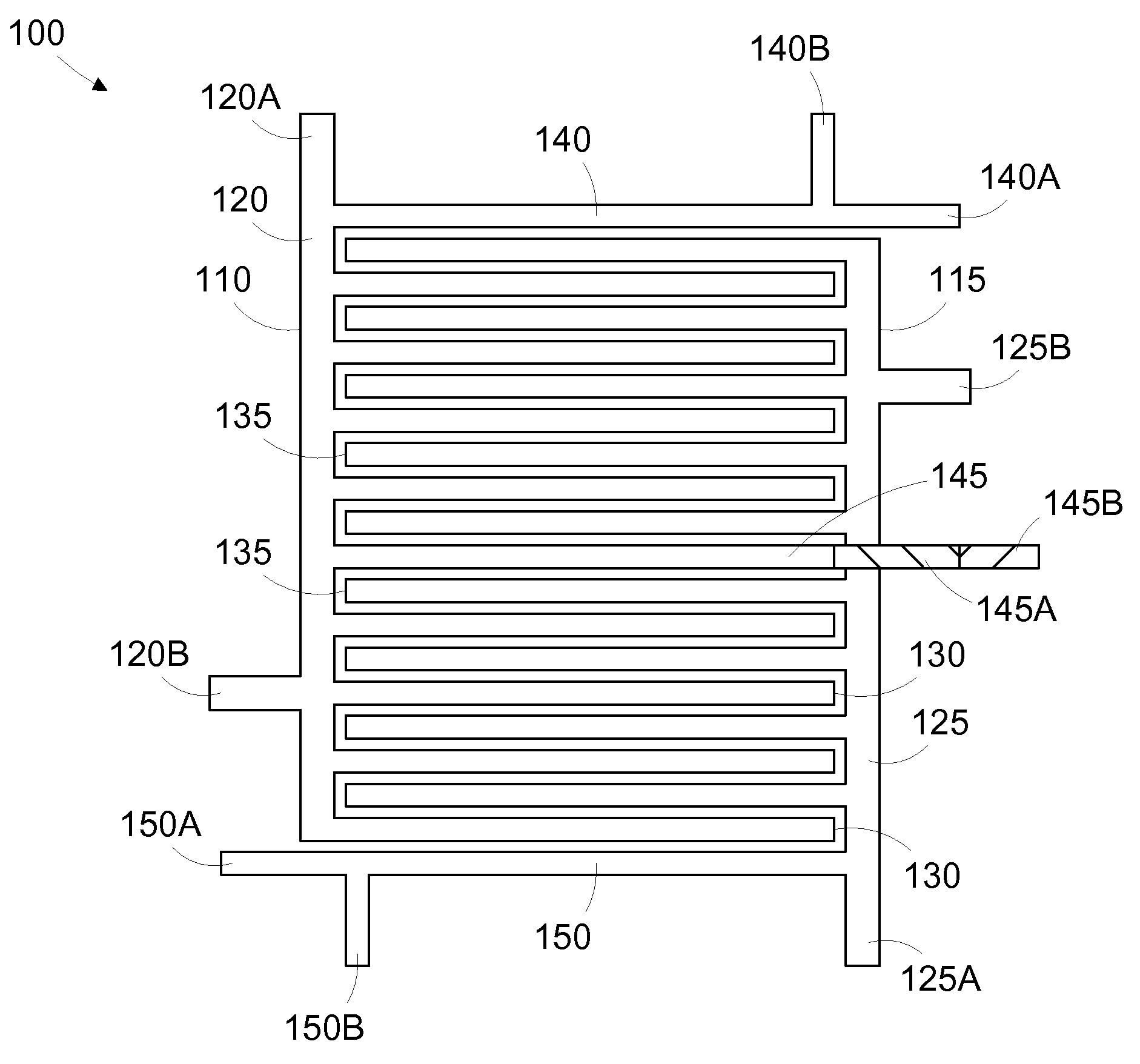
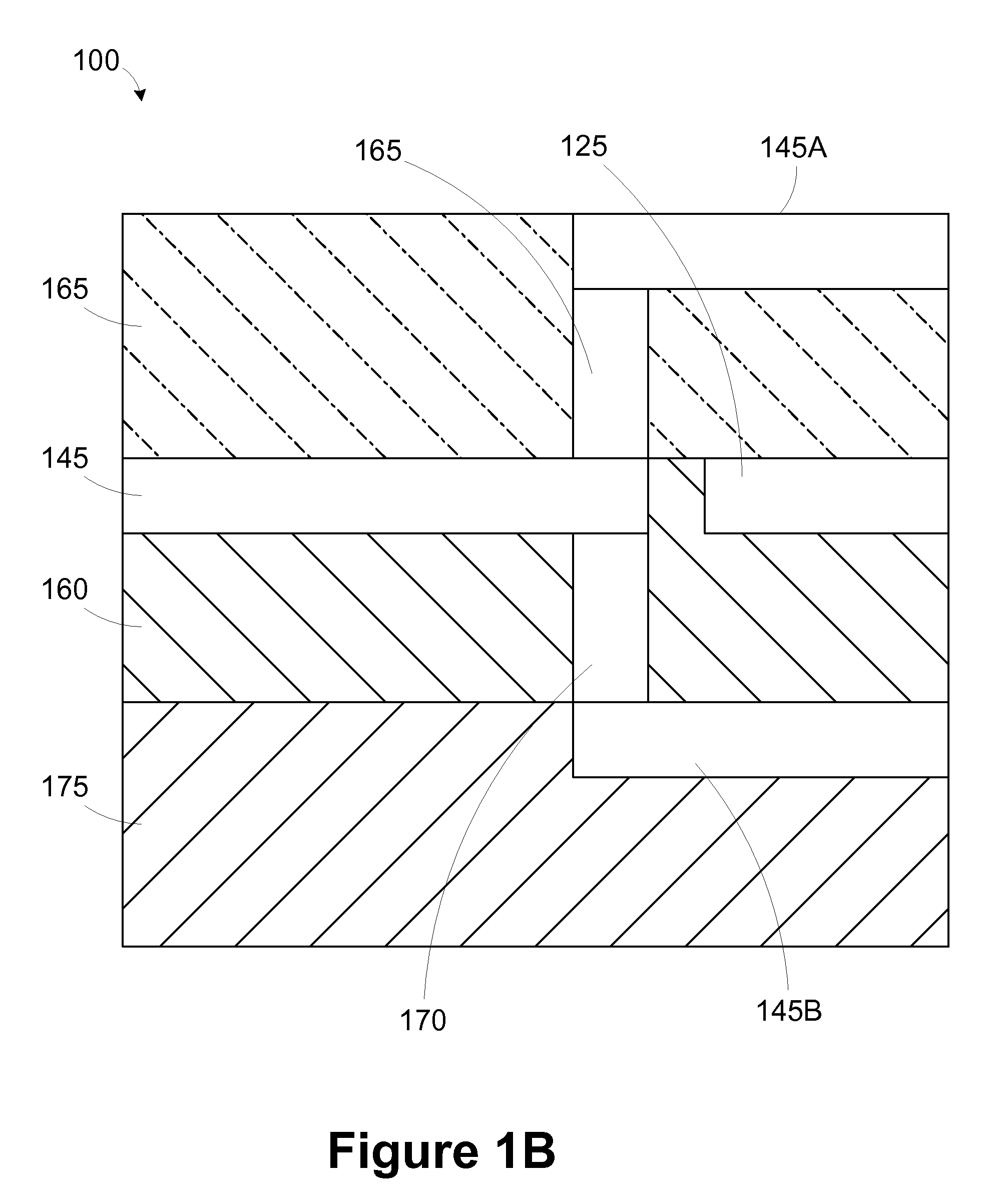
[0021]One or more specific embodiments of the present invention will be described below. It is specifically intended that the present invention not be limited to the embodiments and illustrations contained herein, but include modified forms of those embodiments including portions of the embodiments and combinations of elements of different embodiments as come within the scope of the following claims. It should be appreciated that in the development of any such actual implementation, as in any engineering or design project, numerous implementation-specific decisions must be made to achieve the developers' specific goals, such as compliance with system-related and business related constraints, which may vary from one implementation to another. Moreover, it should be appreciated that such a development effort might be complex and time consuming, but would nevertheless be a routine undertaking of design, fabrication, and manufacture for those of ordinary skill having the benefit of this...


PUM


Abstract

A test structure includes first and second combs, at least a first pair of base nodes, and a second pair of finger nodes. The first comb includes a first base and a first plurality of fingers extending from the first base. The second comb includes a second base and a second plurality of fingers extending from the second base. At least a portion of the first and second pluralities of fingers are interleaved. The first pair of base nodes extend from the first base. The second pair of finger nodes extend from a first finger of the first plurality of fingers.

Description

CROSS-REFERENCE TO RELATED APPLICATIONS[0001]Not applicable.STATEMENT REGARDING FEDERALLY SPONSORED RESEARCH OR DEVELOPMENT[0002]Not applicableBACKGROUND OF THE INVENTION[0003]The present invention relates generally to the field of semiconductor manufacturing and, more particularly, to the use of a test structure for measuring electrical and dimensional characteristics.[0004]A conventional integrated circuit device, such as a microprocessor, is typically comprised of many thousands of semiconductor devices, e.g., transistors, formed above the surface of a semiconductive substrate. For the integrated circuit device to function, the transistors must be electrically connected to one another through conductive interconnect structures. Many modern integrated circuit devices are very densely packed, i.e., there is very little space between the transistors formed above the substrate. Thus, these conductive interconnect structures must be made in multiple layers to conserve plot space on th...

Claims


Application Information

Patent Timeline
Patent Type & Authority Patents(United States)
IPC IPC(8): H01L23/58
CPCG01R31/2884G01R31/2648
Inventor ZHU, JIANHONGWU, DAVID D.MICHAEL, MARK W.
Owner ADVANCED MICRO DEVICES INC
Why Eureka
Try Eureka