

Programmable differential signaling system
a differential signaling and data transmission technology, applied in the field of data communication, can solve the problems of relatively slow data rate, adverse effects on vos and vod, and difficult cmos process
- Summary
- Abstract
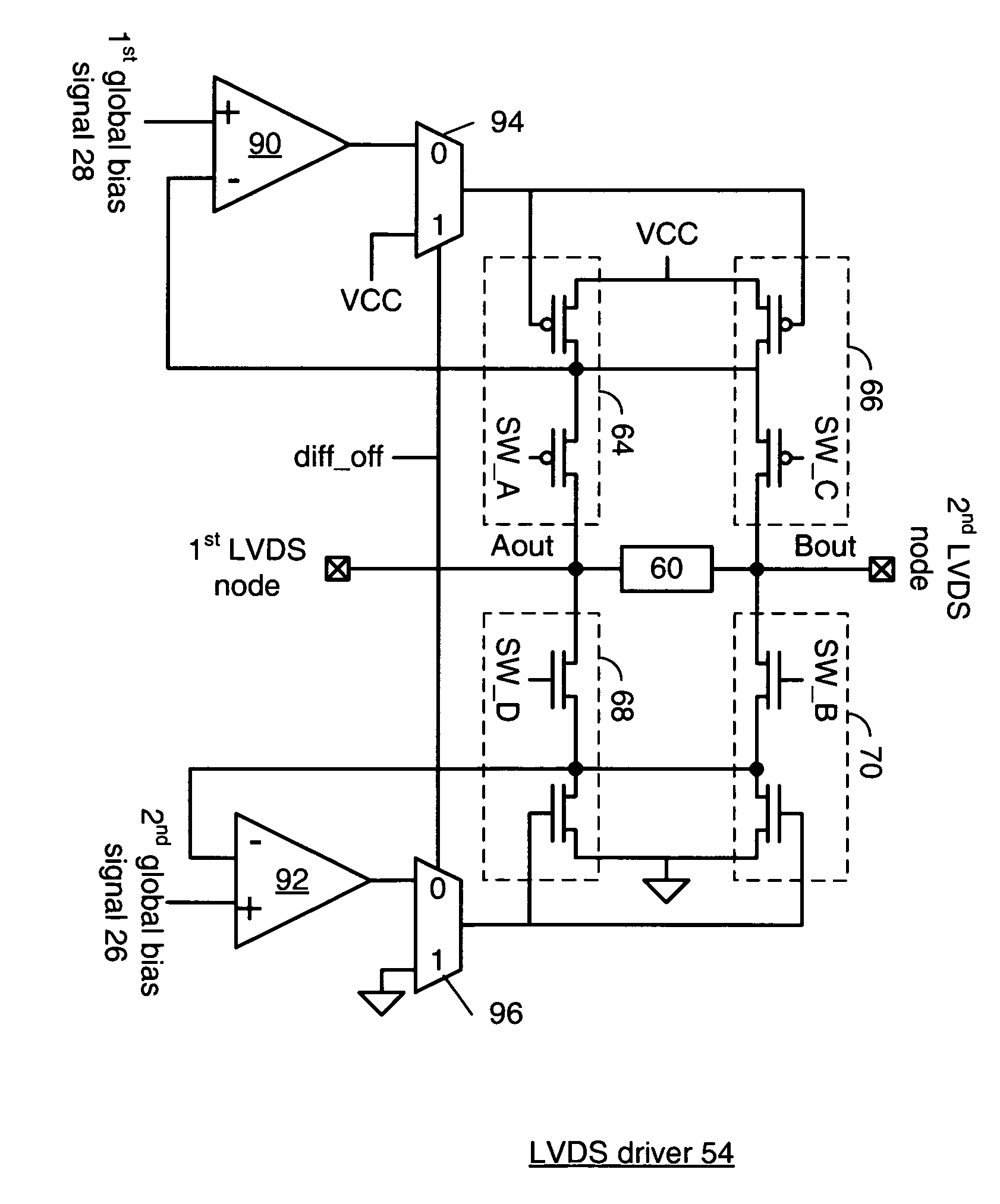
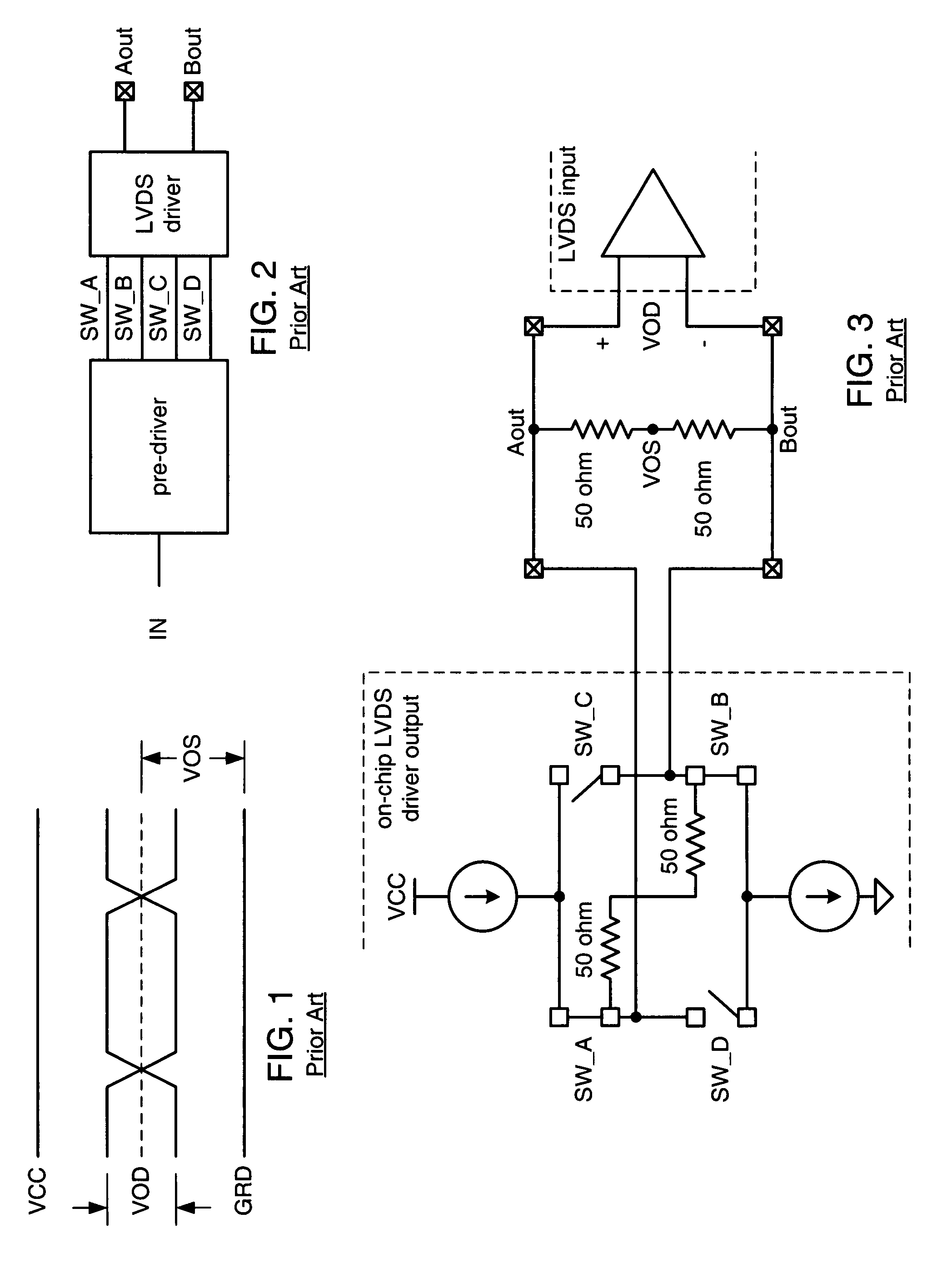
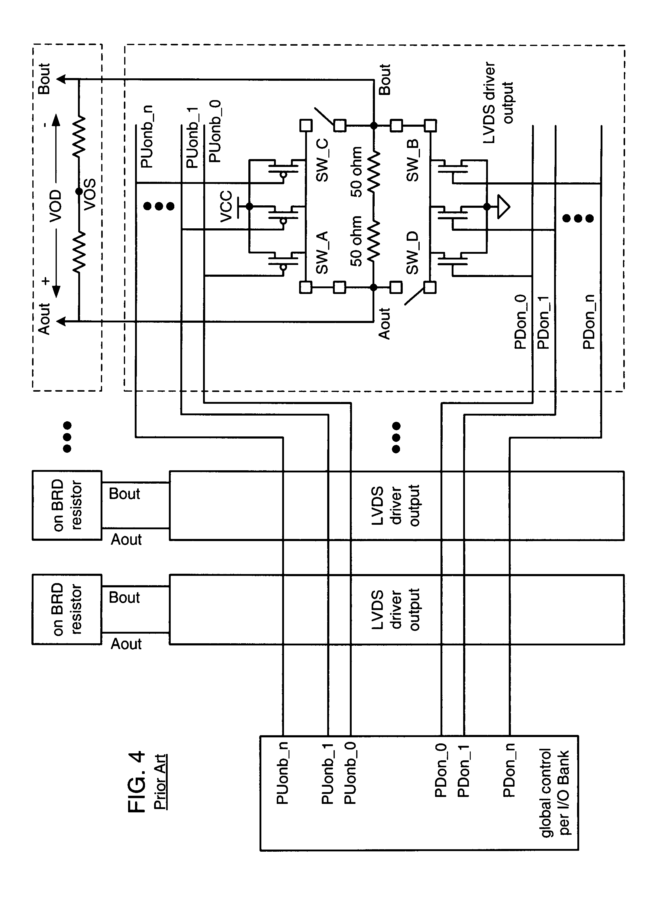
- Description
- Claims
- Application Information
AI Technical Summary
Benefits of technology
Problems solved by technology
Method used
Image

Examples
Embodiment Construction
[0045]FIG. 10 illustrates an FPGA architecture 200 that includes a large number of different programmable tiles including multi-gigabit transceivers (MGTs 201), configurable logic blocks (CLBs 202), random access memory blocks (BRAMs 203), input / output blocks (IOBs 204), configuration and clocking logic (CONFIG / CLOCKS 205), digital signal processing blocks (DSPs 206), specialized input / output blocks (I / O 207) (e.g., configuration ports and clock ports), and other programmable logic 208 such as digital clock managers, analog-to-digital converters, system monitoring logic, and so forth. Some FPGAs also include dedicated processor blocks (PROC 210).
[0046]In some FPGAs, each programmable tile includes a programmable interconnect element (INT 211) having standardized connections to and from a corresponding interconnect element in each adjacent tile. Therefore, the programmable interconnect elements taken together implement the programmable interconnect structure for the illustrated FPGA....
PUM
 Abstract
Description
Claims
Application Information