

Advanced electromagnetic location of electronic equipment
a technology of electronic equipment and location, applied in the field of advanced electromagnetic location of electronic equipment, to achieve the effect of improving accuracy, efficient frequency for further operations, and facilitating the use of radio waves
- Summary
- Abstract
- Description
- Claims
- Application Information
AI Technical Summary
Benefits of technology
Problems solved by technology
Method used
Image

Examples
Embodiment Construction
[0042]Prior to proceeding to the more detailed description of the invention it should be noted that identical components which have identical functions have been designated with identical reference numerals throughout the several views illustrated in the drawings for the sake of clarity.
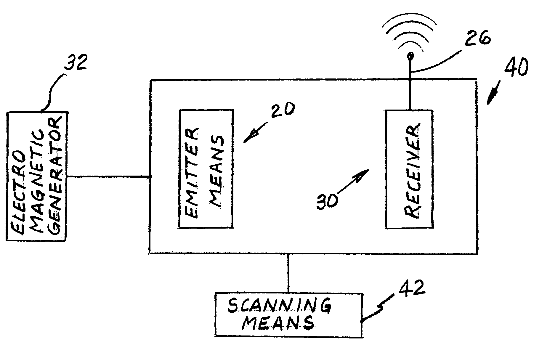
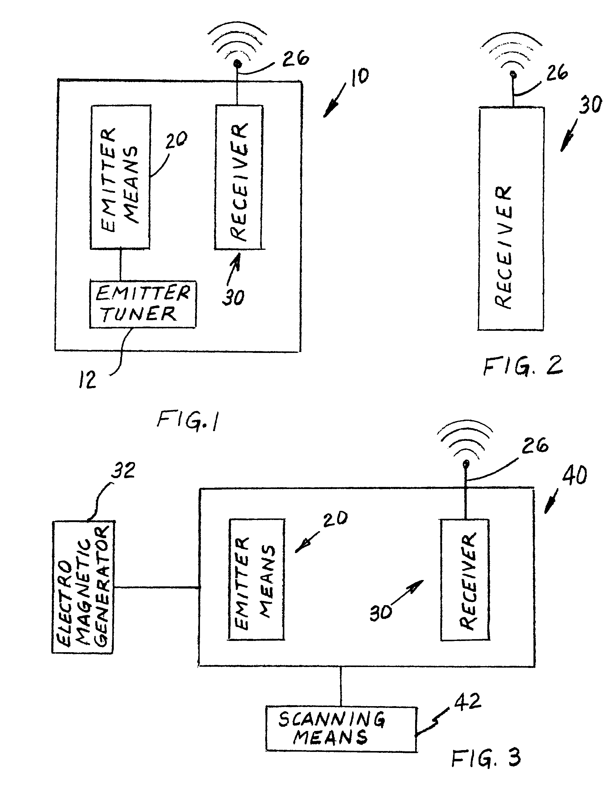
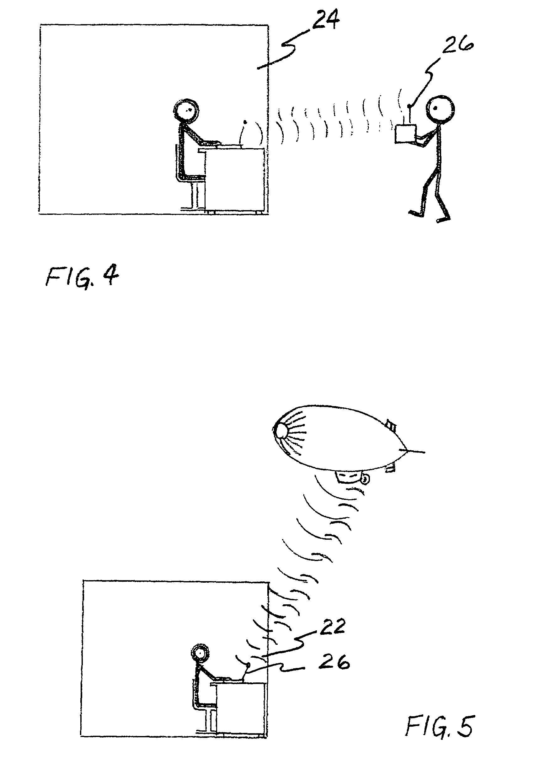
[0043]Now refer more particularly to FIGS. 1 and 2 of the drawings. Illustrated therein is an apparatus, generally designated 10, for measuring at least one of unintentional and intentional electromagnetic emissions for at least one of enabling electromagnetic location of predetermined electronic equipment giving off such at least one of unintentional and intentional electromagnetic emissions, tagging such predetermined electronic equipment and tracking such predetermined electronic equipment and various combination thereof. Apparatus 10 includes an emitter means 20 for providing an amplified electromagnetic energy which at least one of amplifies and changes a frequency content of the at least one of...
PUM
 Abstract
Description
Claims
Application Information