Image device and associated methodology of adjusting a flash exposure operation

a technology of flash exposure and image device, which is applied in the field of imaging apparatus, can solve the problems of improper level of signals and difficulty in accurately determining the amount of main flashing ligh

Inactive Publication Date: 2009-09-15
SONY CORP
View PDF20 Cites 11 Cited by
  • Summary
  • Abstract
  • Description
  • Claims
  • Application Information

AI Technical Summary

Benefits of technology

[0005]The present invention has been made in view of such circumstances, and an object thereof is to provide an imaging apparatus capable of determining the amount of main-flashing light based on pre-flashing by a flash highly accurately, even using an image pickup device formed from a plurality of pixels, each of which can perform any of its exposure operation and reading operation at a timing different from that of the other, such as an XY addressable image sensor, notably a CMOS image sensor.

Problems solved by technology

However, when the imaging apparatus applying a sufficiently long preflash exposure time fires a preflash under ambient light, the amount of light entering a certain zone of the CMOS image sensor may sometimes exceed a dynamic range of the CMOS image sensor, producing image signals exhibiting improper levels from that zone, and thus leaving unsolved the problem of the difficulty in determining the amount of main-flashing light accurately enough.

Method used


Image

  • Image device and associated methodology of adjusting a flash exposure operation
  • Image device and associated methodology of adjusting a flash exposure operation
  • Image device and associated methodology of adjusting a flash exposure operation

Examples


embodiment 1

[0023]An imaging apparatus according to Embodiment 1 of the present invention will be described below with reference to the drawings.

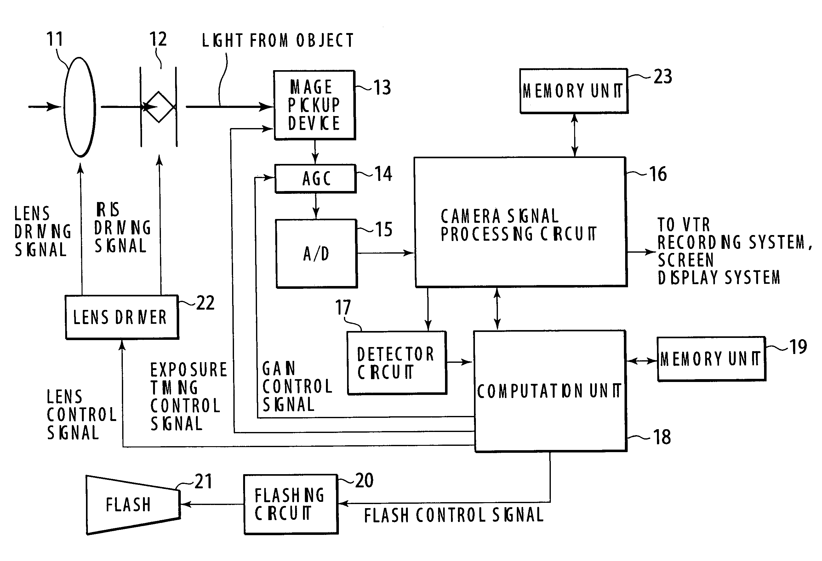
[0024]FIG. 1 is a diagram showing a general configuration of the imaging apparatus according to Embodiment 1.

[0025]As shown in FIG. 1, the imaging apparatus according to Embodiment 1 includes a lens 11, an iris 12, an image pickup device 13, an AGC (Auto Gain Controller) 14, an A / D converter 15, a camera signal processing circuit 16, a detector circuit 17, a computation unit 18, a memory unit 19, a flashing circuit 20, a flash 21, a lens driver 22, and a memory unit 23.

[0026]The lens 11 passes light from an object therethrough for focusing onto the image pickup device 13, during imaging. The iris 12 changes its aperture to optimize the amount of light entering through the lens 11, for the sensitivity of the image pickup device 13. Also, the iris 12 functions as a shutter. The image pickup device 13 includes a plurality of pixels with R, G, B color filt...


PUM


Abstract

An image pickup device and associated methodology are provided. The image pickup device is formed from a plurality of pixels, each of which can perform any of an exposure operation and a reading operation thereof at a timing different from that of the other, an imaging apparatus is provided, which can determine the amount of main-flashing light based on pre-flashing by a flash highly accurately. Before and during a preflash operation by a flash unit, an exposure operation is started simultaneously for all the pixels of the image pickup device 14 to form an image before and during the preflash to obtain a detected value by a detector before and during the preflash, respectively. A computation circuit computes a differential detected value obtained by subtracting the before-preflash detected value from the during-preflash detected value. The differential detected value is a detected value containing only pre-flashed light with ambient light excluded. An amount of light for main flashing is computed on the basis of the differential detected value.

Description

TECHNICAL FIELD[0001]The present invention relates to an imaging apparatus for forming images by firing a flash.BACKGROUND ART[0002]An imaging apparatus is known which, for flash imaging, fires a preflash, and detects reflected light from an object to determine an amount of main-flashing light. Imaging apparatus mainly use a CCD (Charge Coupled Device) image sensor as their image pickup device. Recently, amid the growing trend toward a higher density of pixels on image pickup devices, a CMOS image sensor is drawing attention as a new type of image pickup device. The CMOS image sensor has advantages such as random access to and high-speed reading of pixel signals, high sensitivity, low power consumption, and the like.[0003]However, in a conventional imaging apparatus using a CMOS image sensor, exposure operation and reading operation are performed differently for each pixel, and when a preflash is fired, preflash effects are given only to a part of the image pickup device, posing a p...

Claims


Application Information

Patent Timeline
Patent Type & Authority Patents(United States)
IPC IPC(8): H04N5/222G03B15/03H04N5/335H04N3/14H04N5/235H04N5/238H04N5/353H04N5/374H04N5/376
CPCH04N5/2354G03B15/05G03B2215/05H04N23/74
Inventor CHIBA, TAKUYATANAKA, KAZATOHAYASHI, NAOKI
Owner SONY CORP
Why Eureka
Try Eureka