Coreless thin substrate with embedded circuits in dielectric layers and method for manufacturing the same

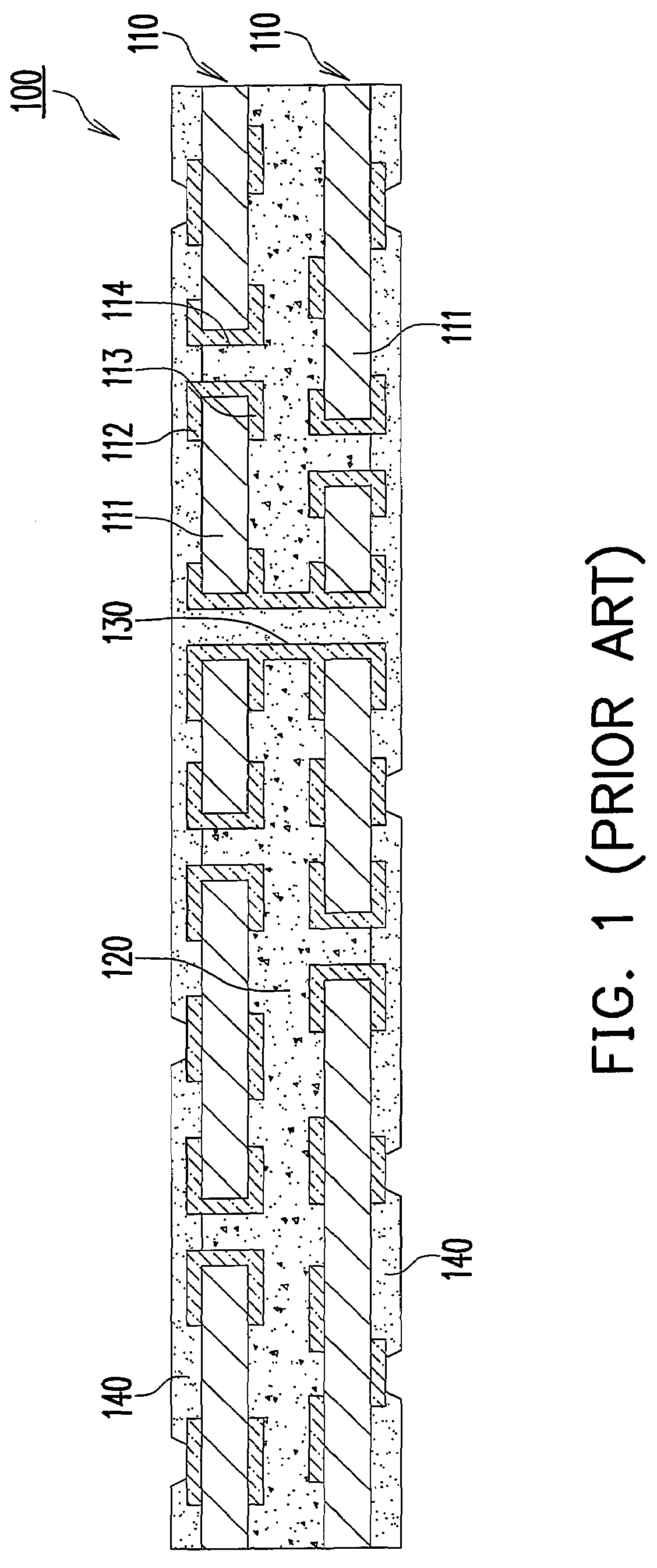
a technology of dielectric layer and coreless thin substrate, which is applied in the direction of resist details, printed circuit aspects, patterning and lithography, etc., can solve the problems of inability to control the thickness of multi-layer circuit boards, disadvantages of flattening and planarization of circuit boards, and inability to control the thickness of insulating layers b>120/b> for electrically insulating different core substrates, etc., to achieve thin and flatter substrates, thin profiles

Active Publication Date: 2010-06-01
ADVANCED SEMICON ENG INC
View PDF3 Cites 17 Cited by
  • Summary
  • Abstract
  • Description
  • Claims
  • Application Information

AI Technical Summary

Benefits of technology

[0009]The present invention is directed to providing a coreless thin substrate with embedded circuits in dielectric layers and a method for manufacturing the same. The substrate comprises a plurality of first patterned dielectric layers with a plurality of embedded circuits, and at least a second patterned dielectric layer with a plurality of embedded conducting elements. The second patterned dielectric layer is disposed between the first patterned dielectric layers, such that the embedded conducting elements electrically conduct the circuits of the first patterned dielectric layers through thermal lamination. Thus, a conventional through-hole formation process after the thermal lamination is skipped, and the substrate has a thinner and flatter profile.
[0010]The present invention is further directed to providing a careless thin substrate with embedded circuits in dielectric layers, a method for manufacturing the same, and a structure of embedded circuits. The first patterned dielectric layers are inkjet printed layers of negative images. The images of the patterns of the first patterned dielectric layers are opposite to the circuits on the same layer, such that the circuits are embedded in the first patterned dielectric layers; and a thickness of the first patterned dielectric layers is the same as a thickness of the circuits embedded in the first patterned dielectric layers, such that the circuits are flush with and exposed from an upper surface and a lower surface of the first patterned dielectric layers, so as to electrically connect the circuits and the embedded conducting elements during the thermal lamination without the complicated substrate process using the conventional core layers.

Problems solved by technology

And after multiple layers of the core layer, the insulating layers, and the circuit layers are formed layer by layer, the thickness of the multi-layer circuit board cannot be controlled, and the surface of the multi-layer circuit board is not planar.
However, in the aforementioned known multi-layer circuit board structures, a core layer is required, and the circuits are protruded from the surface of the core layer, which are disadvantageous to the flattening and planarization of the circuit board.
However, the thickness of the insulating layer 120 for electrically insulating different core substrates 110 cannot be controlled.
As the manufacturing flow of the conventional laminated multi-layer circuit board 100 is complicated, the manufacturing cost is high, and the thickness of the circuit board 100 is great.

Method used


Image

  • Coreless thin substrate with embedded circuits in dielectric layers and method for manufacturing the same
  • Coreless thin substrate with embedded circuits in dielectric layers and method for manufacturing the same
  • Coreless thin substrate with embedded circuits in dielectric layers and method for manufacturing the same

Examples


Embodiment Construction

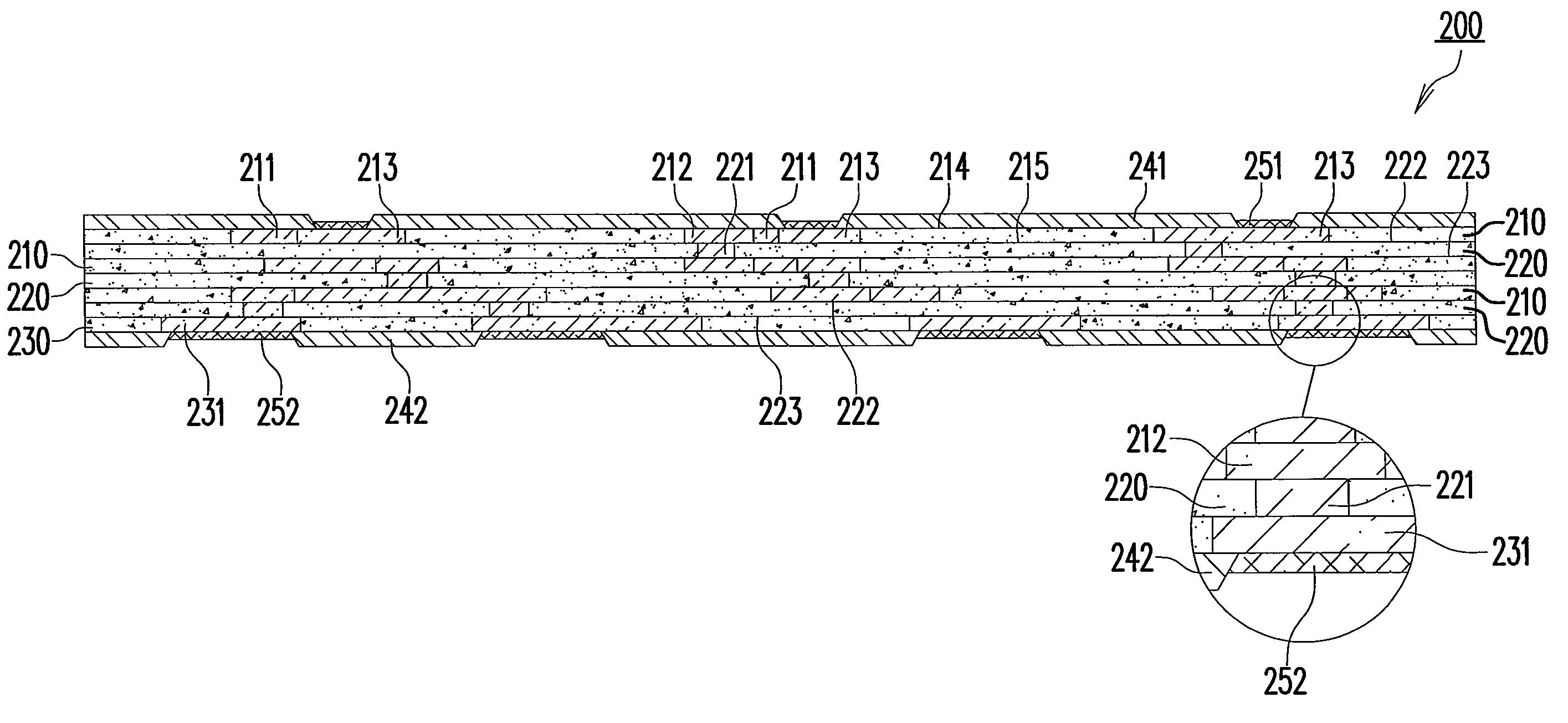
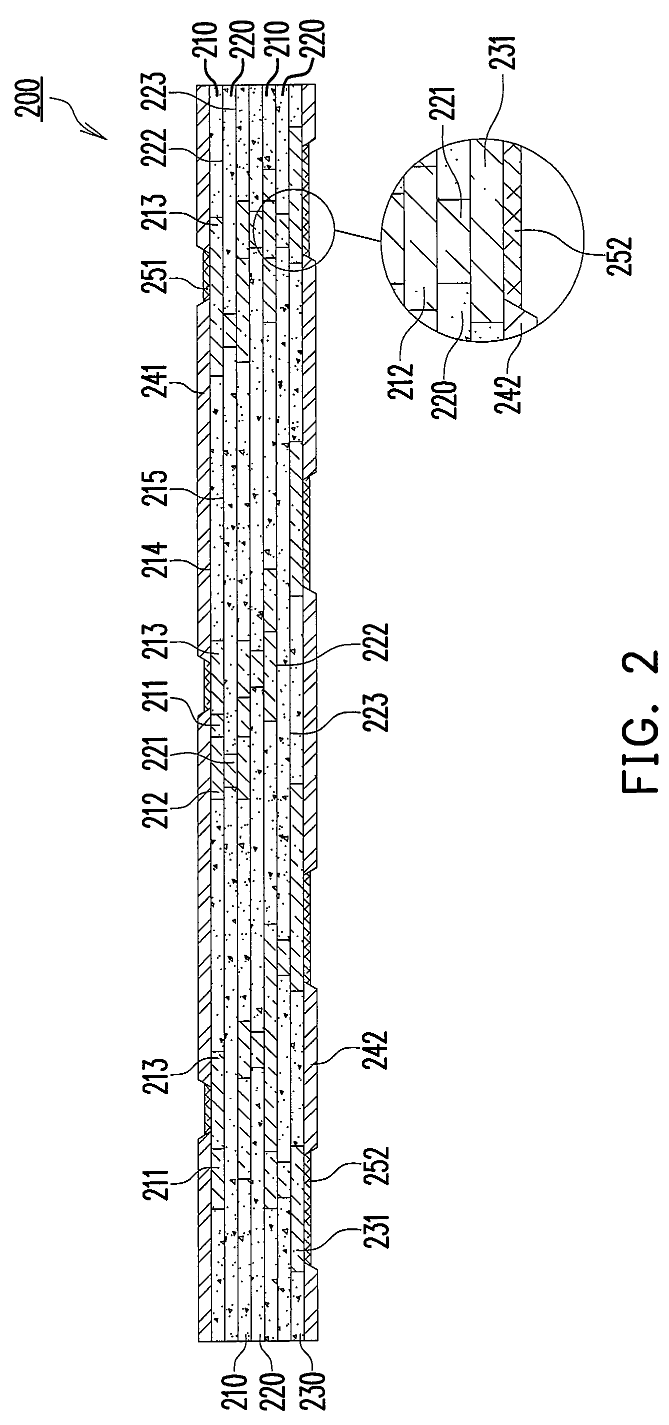
[0017]An embodiment of the present invention is illustrated as follows. As shown in FIG. 2, a coreless thin substrate with embedded circuits in dielectric layers 200 mainly includes a plurality of first patterned dielectric layers 210 and at least a second patterned dielectric layer 220. The second patterned dielectric layer 220 is disposed between the first patterned dielectric layers 210.

[0018]A plurality of circuits 211 is embedded in each of the first patterned dielectric layers 210. The circuits 211 are connected to a plurality of interconnection pads 212, which is also embedded in the first patterned dielectric layers 210. In addition, a plurality of first external connection pads 213 for connecting the circuits 211 is embedded in the outermost first patterned dielectric layer 210. As the circuits 211, the interconnection pads 212, and the first external connection pads 213 are embedded in the first patterned dielectric layers 210, the first patterned dielectric layers 210 hav...


PUM

PropertyMeasurementUnit
thicknessaaaaaaaaaa
thicknessaaaaaaaaaa
non-conductiveaaaaaaaaaa

Abstract

A coreless thin substrate with embedded circuits in dielectric layers is provided. The substrate includes a plurality of first patterned dielectric layers with embedded circuits, and at least a second patterned dielectric layer with embedded conducting elements. The second patterned dielectric layer is disposed between the first patterned dielectric layers, such that the embedded conducting elements electrically conduct the circuits of the first patterned dielectric layers through thermal lamination. Thus, a conventional through-hole formation process after the thermal lamination is skipped, and the substrate has a thinner and flatter profile. In one embodiment, the first patterned dielectric layers are inkjet printed layers with negative images. Moreover, the embedded circuits are flush with and exposed from an upper surface and a lower surface of the corresponding first dielectric layers.

Description

CROSS-REFERENCE TO RELATED APPLICATION[0001]This application claims the priority benefit of Taiwan application serial no. 95111566, filed on Mar. 31, 2006. All disclosure of the Taiwan application is incorporated herein by reference.BACKGROUND OF THE INVENTION[0002]1. Field of Invention[0003]The present invention relates to a multi-layer circuit board. More particularly, the present invention relates to a coreless thin substrate with embedded circuits in dielectric layers and a method for manufacturing the same.[0004]2. Description of Related Art[0005]Multi-layer circuit boards are used in various electronic products for the connection of electrical signal transmission, power supply, and grounding. With the miniaturization of the electronic products, it is required that the multi-layer circuit boards become thinner, and circuits on the multi-layer circuit boards become denser. Generally, the multi-layer circuit boards are classified into lamination circuit board and build-up circuit...

Claims


Application Information

Patent Timeline
Patent Type & Authority Patents(United States)
IPC IPC(8): H01R12/04H05K1/11
CPCH05K3/207H05K3/4617H05K3/125H05K3/1258H05K2203/0568H05K2201/0376H05K2201/10378H05K2203/013
Inventor WANG, CHIEN-HAO
Owner ADVANCED SEMICON ENG INC
Why Eureka
Try Eureka