Check patentability & draft patents in minutes with Patsnap Eureka AI!

Method and apparatus for controlling composition profile of copper indium gallium chalcogenide layers

a composition profile and composition technology, applied in the field of method and apparatus for preparing thin films of semiconductor films, can solve the problems of difficulty in uniform distribution of ga through the thickness of the absorber layer, higher electricity generation cost of silicon-based solar cells than the cost of electricity generated by the more traditional methods, etc., and achieve the effect of increasing the performance of such absorbers and low efficiencies

Inactive Publication Date: 2010-12-21
SOLOPOWER
View PDF12 Cites 5 Cited by
  • Summary
  • Abstract
  • Description
  • Claims
  • Application Information

AI Technical Summary

Benefits of technology

The method ensures a substantially uniform Ga distribution throughout the absorber layer, enhancing the solar cell's open circuit voltage and overall efficiency, potentially reaching higher performance levels similar to co-evaporation processes.

Problems solved by technology

However, the cost of electricity generated using silicon-based solar cells is higher than the cost of electricity generated by the more traditional methods.
Referring back to curve A in FIG. 2, one problem faced with the selenization type processes (also called two-stage processes) is the difficulty to distribute Ga uniformly through the thickness of the absorber layer formed after reaction of metallic precursor film with Se.
Therefore, such a process yields compound absorber layers with surfaces that are rich in In and poor in Ga.

Method used


Image

  • Method and apparatus for controlling composition profile of copper indium gallium chalcogenide layers
  • Method and apparatus for controlling composition profile of copper indium gallium chalcogenide layers
  • Method and apparatus for controlling composition profile of copper indium gallium chalcogenide layers

Examples


Embodiment Construction

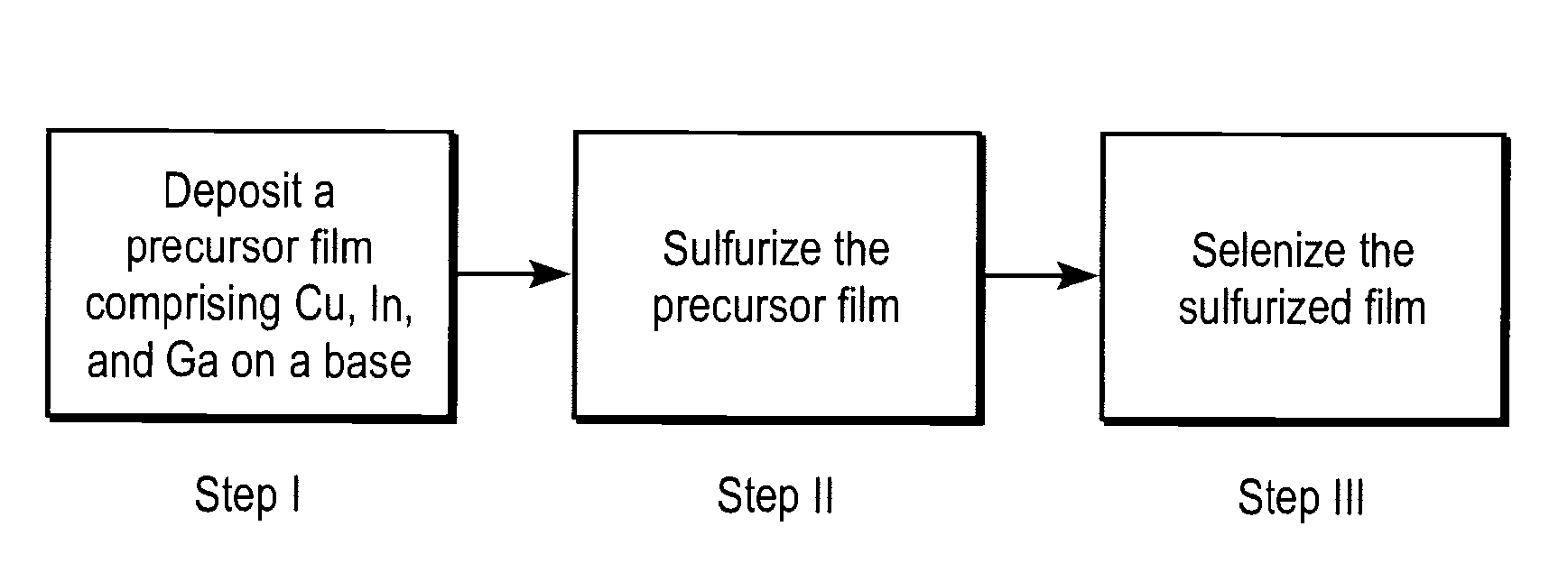
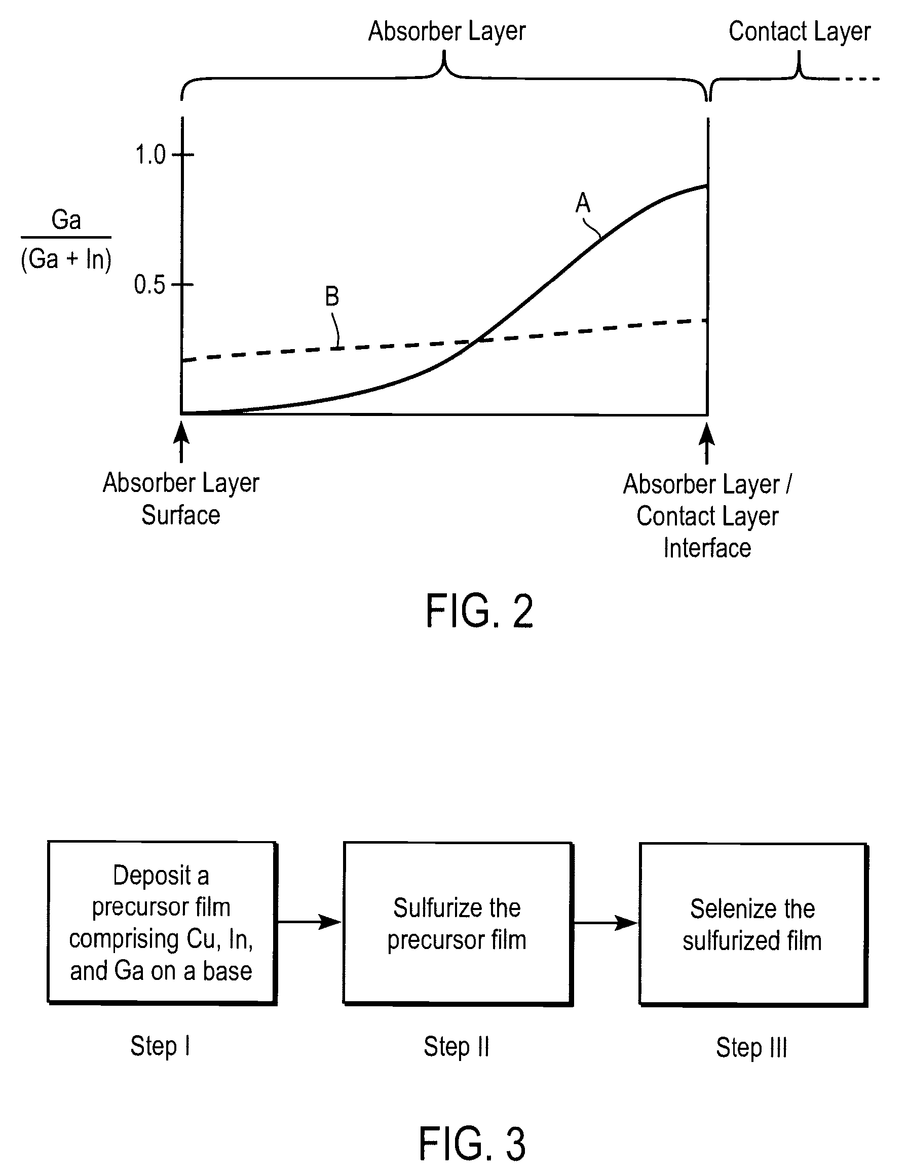
[0018]FIG. 3 shows the process steps for growing a Cu(In,Ga)Se2 absorber layer on a base, wherein the Ga distribution within the absorber layer is substantially uniform. As can be seen from FIG. 3, the first step of the process (Step I) is deposition of a precursor film on a base, the precursor film preferably including Cu, In and Ga. As an example, the amounts of Cu, In and Ga may be such that Cu / (In+Ga) molar ratio in the film may be in the range of 0.7-1.0, preferably in the range of 0.8-0.9, and the Ga / (Ga+In) molar ratio may be in the range of 0.1-0.5, preferably in the range of 0.2-0.35. The precursor film may be deposited on the base by a variety of techniques such as electrodeposition, evaporation, sputtering, ink deposition etc. The precursor film may include nano particles made of Cu and / or In and / or Ga and / or their mixtures and / or alloys. Alternately, the precursor film may include at least two sub-layers, each sublayer including at least one of Cu, In and Ga.

[0019]Referr...


PUM

PropertyMeasurementUnit
molar ratioaaaaaaaaaa
temperatureaaaaaaaaaa

Abstract

The present invention relates to method and apparatus for preparing thin films of semiconductor films for radiation detector and photovoltaic applications. In one aspect, the present invention is directed to a method of forming a Cu(In,Ga)(S,Se)2 layer with substantially uniform Ga distribution. In a particular aspect, the method includes depositing a precursor film on the base, the precursor film including Cu, In and Ga, sulfurizing the precursor film thus forming a sulfurized precursor layer with a substantially uniform Ga distribution, and selenizing the sulfurized precursor layer to reduce the sulfur concentration therein and obtain the Cu(In,Ga)(S,Se)2 layer with substantially uniform Ga distribution. In a further aspect, the method also includes the step of selenizing the precursor film.

Description

CLAIM OF PRIORITY[0001]This application claims priority to U.S. Provisional Appln. Ser. No. 60 / 862,164 filed Oct. 19, 2006 entitled “Roll-To-Roll Electroplating For Photovoltaic Film Manufacturing”, U.S. Provisional Appln. Ser. No. 60 / 865,385 filed Nov. 10, 2006 entitled “Reel-To-Reel Reaction of Precursor Film to Form Solar Cell Absorber”, and U.S. patent application Ser. No. 11 / 549,590 filed Oct. 13, 2006 now abandoned entitled “Method and Apparatus For Converting Precursor Layers Into Photovoltaic Absorbers” and expressly incorporates each of these applications by reference herein.FIELD OF THE INVENTION[0002]The present invention relates to method and apparatus for preparing thin films of semiconductor films for radiation detector and photovoltaic applications.BACKGROUND[0003]Solar cells are photovoltaic devices that convert sunlight directly into electrical power. The most common solar cell material is silicon, which is in the form of single or polycrystalline wafers. However, t...

Claims


Application Information

Patent Timeline
Patent Type & Authority Patents(United States)
IPC IPC(8): B05D3/02H01L21/00
CPCC23C14/14C23C14/5866H01L21/02614H01L31/0322H01L21/02568Y02E10/541
Inventor BASOL, BULENT M.
Owner SOLOPOWER
Features
  • R&D
  • Intellectual Property
  • Life Sciences
  • Materials
  • Tech Scout
  • Unparalleled Data Quality
  • Higher Quality Content
  • 60% Fewer Hallucinations
Learn More