Display device and manufacturing method thereof

a technology of a display device and a manufacturing method, applied in the field of display devices, can solve the problems of uneven image quality uneven amplitude of effective voltage applied to the liquid crystal layer of each pixel, etc., and achieve the effect of decreasing the number of apertures, uneven image quality, and uneven image quality

Active Publication Date: 2011-05-17
PANASONIC INTELLECTUAL PROPERTY CORP OF AMERICA +1
View PDF3 Cites 2 Cited by
  • Summary
  • Abstract
  • Description
  • Claims
  • Application Information

AI Technical Summary

Benefits of technology

[0012]Thus the object of the present invention is to provide for example a technology which allows effectively decreasing the uneven image quality in the liquid crystal display device.
[0013]Another object of the present invention is to provide for example a technology which allows effectively decreasing the uneven image quality without decreasing the number of aperture in the liquid crystal display device.
[0057]wherein in the fifth process step the plan size of the source electrode is determined by providing a part which overlaps with the scan signal line and is branched from the extending direction of the source electrode connecting the part in contact with the source region of the semiconductor layer with the part connecting to the pixel electrode, between the part in contact with the source region of the scan signal line and the part connecting to the pixel electrode in the each source electrode, so as to narrow the surface area of the branching part when the distance from one edge of the scan signal line to the semiconductor layer is longer, or so as to enlarge the surface area of the branching part when the distance from one edge of the scan signal line to the semiconductor layer is shorter, in order to evenly form the plan surface area of the overlap region overlapping each source electrode with each scan signal line when viewing in plan view from the top.
[0067]wherein the plan size of the pixel electrode is determined in the sixth process step so as to narrow the surface area of the plan overlap region of the pixel electrode to be connected to the source electrode overlapping with the scan signal line when the surface area of the plan overlap region of the source electrode overlapping with the scan signal line is wider, and so as to enlarge the surface area of the plan overlap region of the pixel electrode to be connected to the source electrode overlapping with the scan signal line when the surface area of the plan overlap region of the source electrode overlapping with the scan signal line is narrower.
[0068]In accordance with the display device of the present invention and the manufacturing method thereof, the wiring capacitance (parasitic capacitance) generated between a scan signal line and the source electrode of a TFT in each pixel forming one display area may be almost evenly formed to allow decreasing the uneven image quality caused by the difference of the amplitude of the wiring capacitance. In addition the difference between plural display devices manufactured from plural TFT substrates obtained from one single mother glass may also be decreased.
[0069]In addition, in accordance with the display device of the present invention and the manufacturing method thereof, the uneven image quality caused by the difference of wiring capacitance between the scan signal line and the source electrode of the TFT may be decreased without decreasing the number of aperture.

Problems solved by technology

However, in the manufacturing method of the TFT substrate in the prior art, for example, there may be a considerable variation in the wiring capacity (parasitic capacity) generated between a source electrode and a scan signal line in a TFT of each pixel, often causing some difference in the amplitude of effective voltage applied to the liquid crystal layer of each pixel.
This may cause a problem of unequal brightness (uneven image quality) within one display area in the large liquid crystal display device.
This may also cause a problem of difference of image quality between two liquid crystal display devices in the small size liquid crystal display device.
However, when widening the width of scan signal lines, another problem of the decreased number of aperture may arise.

Method used


Image

  • Display device and manufacturing method thereof
  • Display device and manufacturing method thereof
  • Display device and manufacturing method thereof

Examples


first embodiment

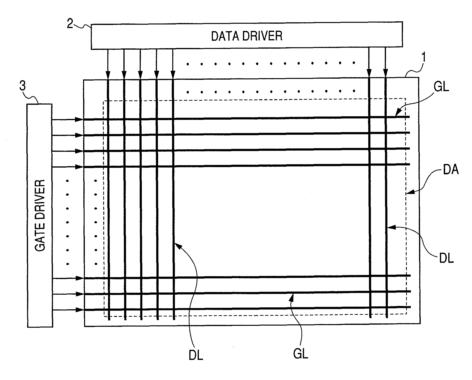
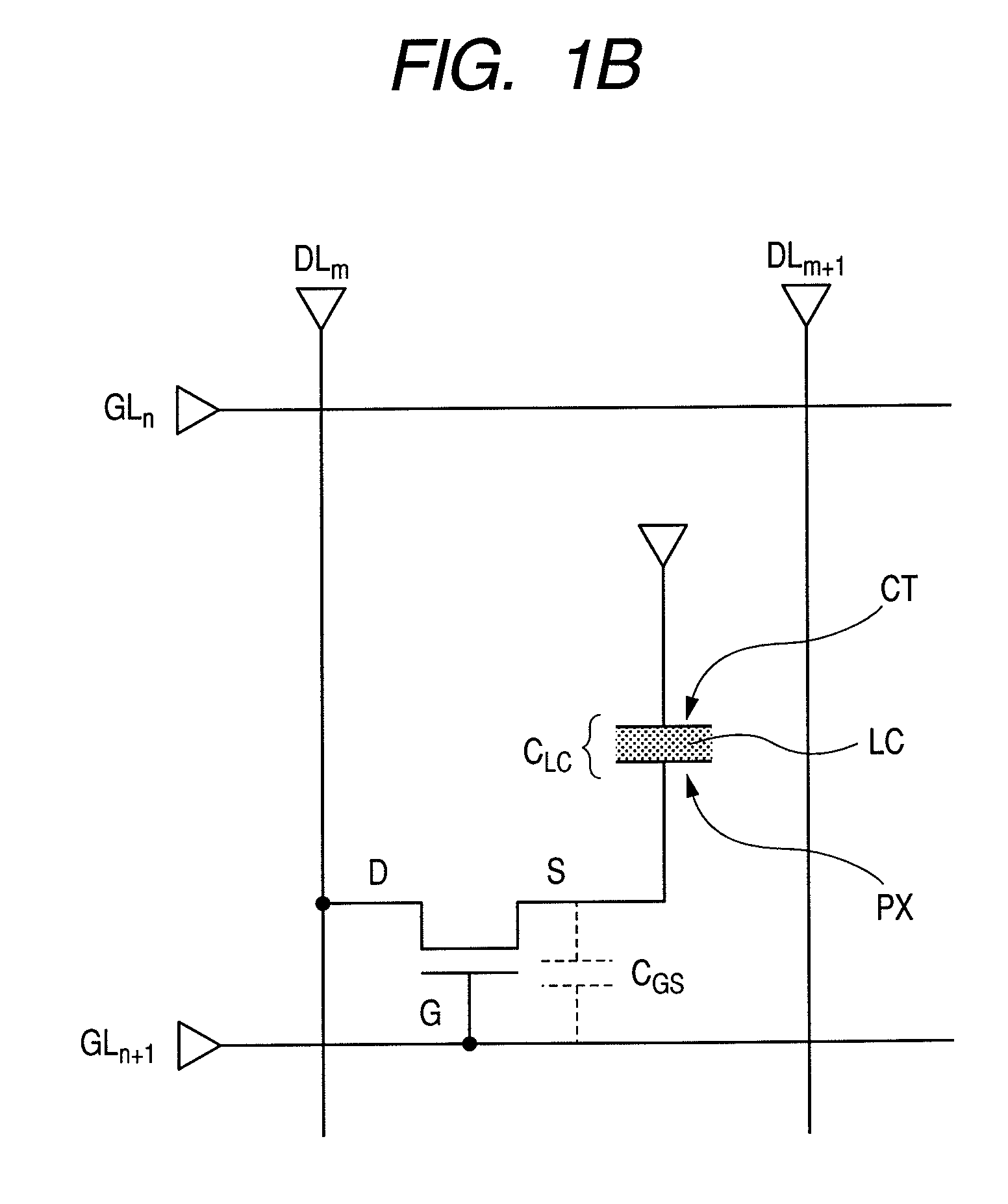
[0086]Now referring to FIGS. 1A and 1B, FIG. 1A shows a schematic diagram illustrating a typical example of the arrangement of a liquid crystal display device in accordance with the present invention. FIG. 1B shows a schematic circuit diagram illustrating the circuit of one pixel in the liquid crystal display panel shown in FIG. 1A.

[0087]The present invention may be applied to a TFT liquid crystal display device of the active matrix type. The active matrix TFT liquid crystal display device has for example a liquid crystal display panel 1, a data driver 2, and a gate driver 3, as shown in FIG. 1A. As is not shown in FIG. 1A, the TFT liquid crystal display device further includes for example a controller circuit for controlling the operation of the data driver 2 and the gate driver 3. The transmissive and semi-transmissive TFT liquid crystal display device has also a backlight unit (light source) as well.

[0088]The liquid crystal display panel 1 has plural scan signal lines GL and plur...

second embodiment

[0151]Now referring to FIGS. 8A to 8D, FIG. 8A shows a schematic plan view illustrating the fundamental arrangement of a TFT in accordance with a second preferred embodiment of the present invention. FIG. 8B shows a schematic plan view illustrating first feature of the TFT substrate in accordance with the second preferred embodiment of the present invention. FIG. 8C shows a schematic plan view illustrating second feature of the TFT substrate in accordance with the second preferred embodiment of the present invention. FIG. 8D shows a schematic diagram illustrating the relationship between the width of scan signal line and the surface area of branch section of the source electrode in the TFT substrate in accordance with the second preferred embodiment of the present invention.

[0152]In the first embodiment, by displacing the semiconductor layer SC, the edge of the drain electrode SD1 opposing to the source electrode SD2, and the edge of the source electrode SD2 opposing to the drain el...

third embodiment

[0182]Now referring to FIGS. 10A and 10B, FIG. 10A shows a schematic plan view illustrating an exemplary arrangement of one pixel in a TFT substrate in accordance with third preferred embodiment of the present invention. FIG. 10B shows a schematic cross-sectional view taken along with the line D-D′ of FIG. 10A. FIG. 10C shows a schematic cross-sectional view taken along with the line E-E′ of FIG. 10A.

[0183]In the first and second preferred embodiments the surface area SGS of the overlap region overlapping the source electrode SD2 with the scan signal line GL in plan view is adjusted so as to adjust the fluctuation of the wiring capacitance formed between the source electrode SD2 and the scan signal line GL.

[0184]In the third preferred embodiment, which is different from the first and second preferred embodiments, a method of adjusting the fluctuation of wiring capacitance formed between the source electrode SD2 and the scan signal line GL by using the pixel electrode PX connected to...


PUM

PropertyMeasurementUnit
DAaaaaaaaaaa
widthaaaaaaaaaa
surface areaaaaaaaaaaa

Abstract

The present invention allows decreasing the uneven image quality in a liquid crystal display device. The display device in accordance with the present invention includes plural scan signal lines, plural video signal lines, plural TFTs placed in a matrix structure, and plural pixel electrodes, when the width of the scan signal line in a region to place one TFT is different from the width of the scan signal line in a region to place another TFT which is different from the one TFT, the channel width and the channel length of the one TFT is almost equal to the channel width and the channel length of the another TFT, and the surface area of the region overlapping the source electrode with the scan signal line of the one TFT when viewing in plan view is almost equal to the surface area of the region overlapping the source electrode with the scan signal line of the another TFT when viewing in plan view.

Description

CLAIM OF PRIORITY[0001]The present application claims priority from Japanese Application JP 2007-008310 filed on Jan. 17, 2007, the content of which is hereby incorporated by reference into this application.BACKGROUND OF THE INVENTION[0002]The present invention is related to a display device and a manufacturing method thereof, in particular to a technology effectively applied to a TFT (thin film transistor) liquid crystal display device and the manufacturing method of the same.[0003]In the liquid crystal display device, there is an active matrix type liquid crystal display device in which active elements (also referred to as switching elements) are placed as matrix. For the active elements as described above TFT of MIS structure (including MOS structure) is used.[0004]The active elements (TFT) in the active matrix type liquid crystal display device may have for example a semiconductor layer on the scan signal lines with a first insulation layer (gate insulation film) interposed ther...

Claims


Application Information

Patent Timeline
Patent Type & Authority Patents(United States)
IPC IPC(8): G02F1/1343H01L27/088G02F1/1368
CPCG02F1/136286H01L27/124G02F1/1368G02F2201/40G02F2001/13606G02F1/13606
Inventor OHARA, KENNAKAYOSHI, YOSHIAKIYAMAMOTO, TSUNENORIEDO, SUSUMU
Owner PANASONIC INTELLECTUAL PROPERTY CORP OF AMERICA
Why Eureka
Try Eureka