Organic light-emitting device

a light-emitting diode and organic technology, applied in the manufacture of electrode systems, electric discharge tubes/lamps, discharge tubes luminescnet screens, etc., can solve the problems of unsatisfactory driving voltage, efficiency, life span, and efficiency of conventional organic light-emitting diodes, and achieve the effect of improving efficiency, power consumption properties, and life span

Active Publication Date: 2011-05-31
SAMSUNG DISPLAY CO LTD
View PDF19 Cites 1 Cited by
  • Summary
  • Abstract
  • Description
  • Claims
  • Application Information

AI Technical Summary

Benefits of technology

[0008]Aspects of the present invention provide an organic light-emitting device with improved life span, efficiency, and power consumption properties compared to devices of the prior art.

Problems solved by technology

However, conventional organic light-emitting diodes do not have satisfactory driving voltage, efficiency, and life span, and thus, improvements are desirable.

Method used


Image

  • Organic light-emitting device
  • Organic light-emitting device
  • Organic light-emitting device

Examples


example

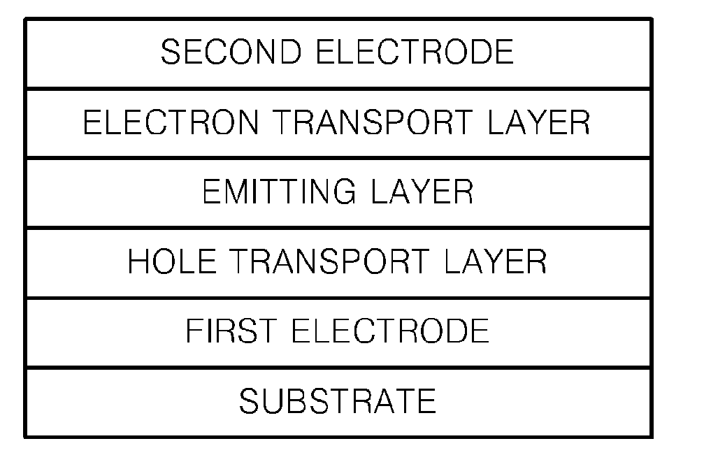
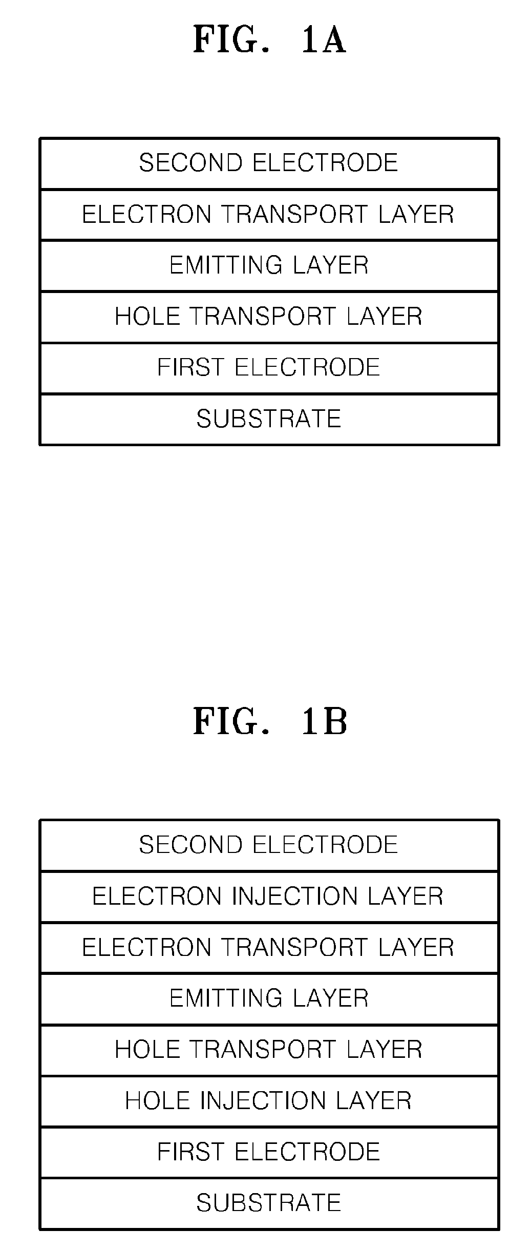
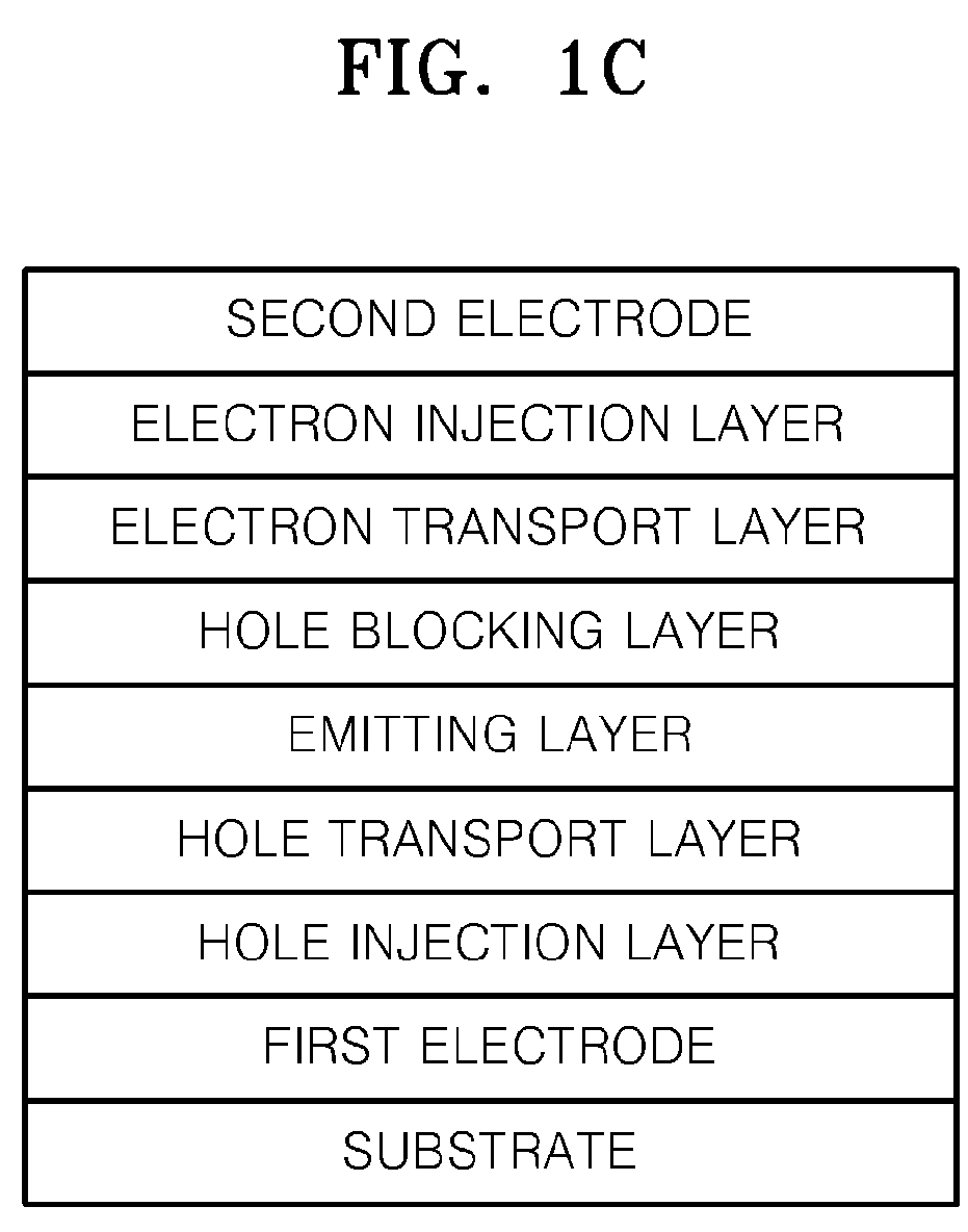
[0066]An anode was prepared and used by cutting a Corning 15 Ωcm2 (1200 Å) Ag / ITO (Ag:ITO=100 nm:7 nm) glass substrate into a size of 50 mm×50 mm×0.7 mm, and sonicating for 5 minutes using isopropyl alcohol and deionized water. The anode was irradiated with UV light for 30 minutes and exposed to ozone to clean, and then was inserted into a vacuum depositing apparatus.

[0067]A hole injecting material by LUDIS Co. (commercial name: LHT-001) was then vacuum deposited on the anode to form a HIL having a thickness of 130 nm. Next, a hole transporting material by Hodokaya Co. (commercial name: EL-301) was vacuum deposited on the HIL to form a HTL having a thickness of 80 nm.

[0068]In order to provide a hole injection material having a reduced amount of impurities, the LHT-001 hole injecting material was synthesized using a Pd-based catalyst instead of a Cu-based catalyst, and the reagents used in the synthesis of the LHT-001 were all reagent grade reagents of 99% purity or higher, sold by A...


PUM

PropertyMeasurementUnit
thicknessaaaaaaaaaa
thicknessaaaaaaaaaa
thicknessaaaaaaaaaa

Abstract

An organic light-emitting device includes a substrate; a first electrode; a second electrode facing the first electrode; an organic layer disposed on the first electrode; and an emitting layer interposed between the organic layer and the second electrode. The concentration of inorganic impurities within the organic layer is 1000 ppb or less. The organic light-emitting device has high light-emitting efficiency, low driving voltage, high brightness, and long life span.

Description

CROSS-REFERENCE TO RELATED APPLICATION[0001]This application claims the benefit of Korean Application No. 2008-20078, filed Mar. 4, 2008, in the Korean Intellectual Property Office, the disclosure of which is incorporated herein by reference.BACKGROUND OF THE INVENTION[0002]1. Field of the Invention[0003]Aspects of the present invention relate to an organic light-emitting device, and more particularly, to an organic light-emitting device including an organic layer having a relatively low concentration of inorganic impurities.[0004]2. Description of the Related Art[0005]Organic light emitting diodes are self light-emitting devices having a wide viewing angle, excellent contrast, and a quick response time, and thus have received much attention. Moreover, organic light emitting diodes have excellent driving voltage and response speed characteristics, and can form multi-colored images.[0006]Organic light emitting diodes conventionally have a stacked structure of anode / emitting layer / cat...

Claims


Application Information

Patent Timeline
Patent Type & Authority Patents(United States)
IPC IPC(8): H01L51/50H01L51/56
CPCH01L51/5088H01L51/004H10K85/141H10K50/17H05B33/18
Inventor CHUN, MIN-SEUNGKIM, DONG-HUNKIM, MI-KYUNGSON, JUNG-HAKWAK, JAE-HYUN
Owner SAMSUNG DISPLAY CO LTD
Why Eureka
Try Eureka