Method of making a molded interconnect device

a technology of interconnection device and molded material, which is applied in the direction of printed circuit manufacturing, printed circuit aspects, conductive pattern formation, etc., can solve the problems of high production cost, environmental pollution, high production cost due to expensive cvd or sputtering tools, etc., and achieve the effect of clean and cost-effectiv

Inactive Publication Date: 2011-10-11
UNIMICRON TECH CORP
View PDF10 Cites 12 Cited by
  • Summary
  • Abstract
  • Description
  • Claims
  • Application Information

AI Technical Summary

Benefits of technology

[0011]It is one objective of the present invention to provide an improved method of making a molded interconnect device, which is clean and cost-effective, in order to solve the above-mentioned prior art problems.

Problems solved by technology

The shortcomings of this method include high production cost due to expensive metal catalyst impregnated plastics and laser tools, and environmental pollution issues due to wet chemical process.
The shortcomings of this method include high production cost due to expensive CVD or sputtering tool as well as environmental pollution issues due to wet chemical process.
One of the drawbacks is that the cost of developing molds is high.
Besides, there are difficulties of three-dimensional processing.
The drawbacks include bottleneck of mold development, low design flexibility and high cost of development.

Method used


Image

  • Method of making a molded interconnect device
  • Method of making a molded interconnect device
  • Method of making a molded interconnect device

Examples


Embodiment Construction

[0018]As previously mentioned, either LDS method or MIPTEC method has a drawback in that the production cost is too high because of the expensive metal impregnated plastic and expensive production tools, and that the employed wet chemical processes have environmental issues. To solve these problems, the present invention discloses a novel and eco-friendly method of making a molded interconnect device, which is cost-effective and is applicable to various injection molded plastic structures to form metallized circuit traces on any surface of the injection molded plastic structure.

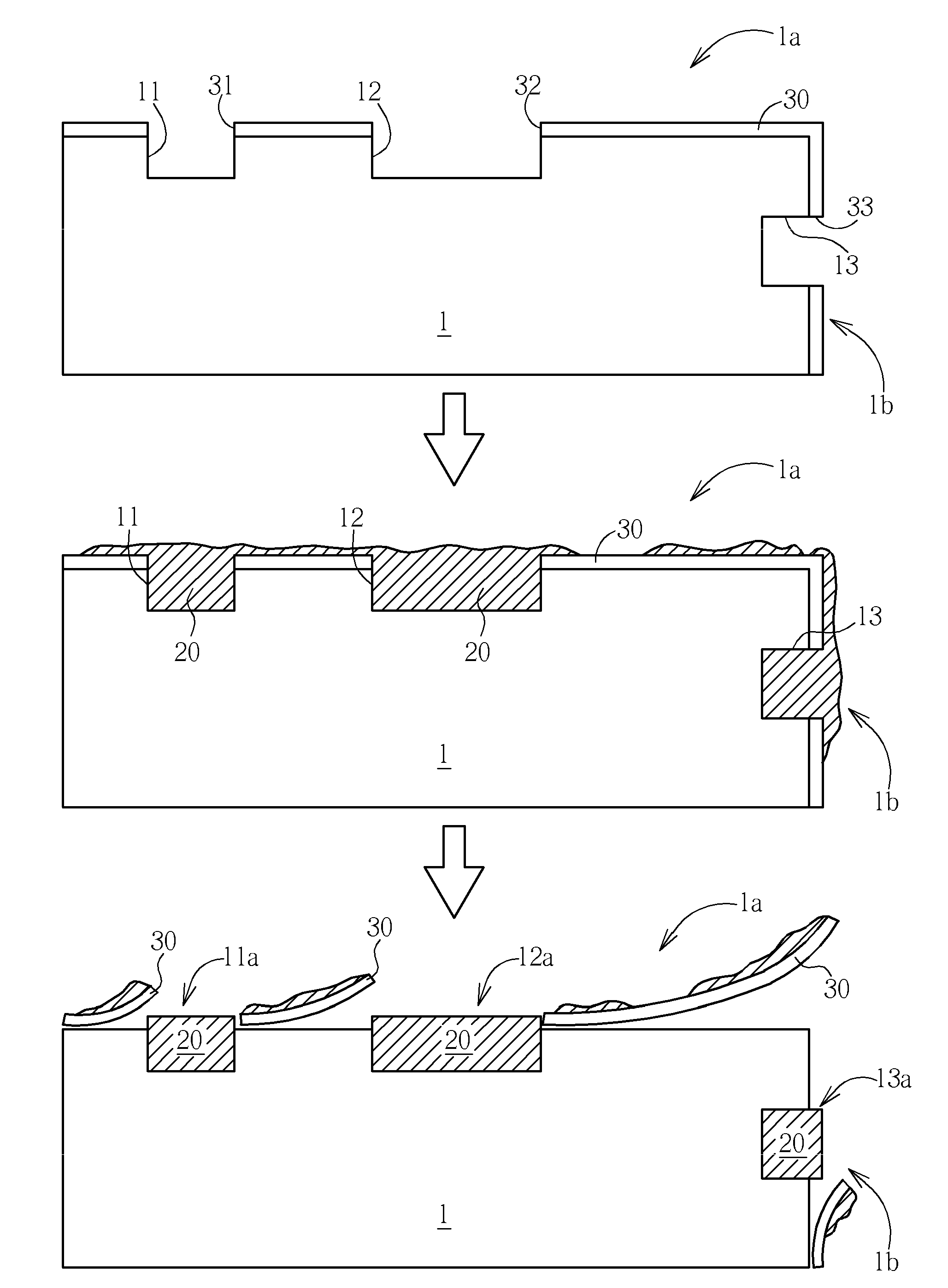
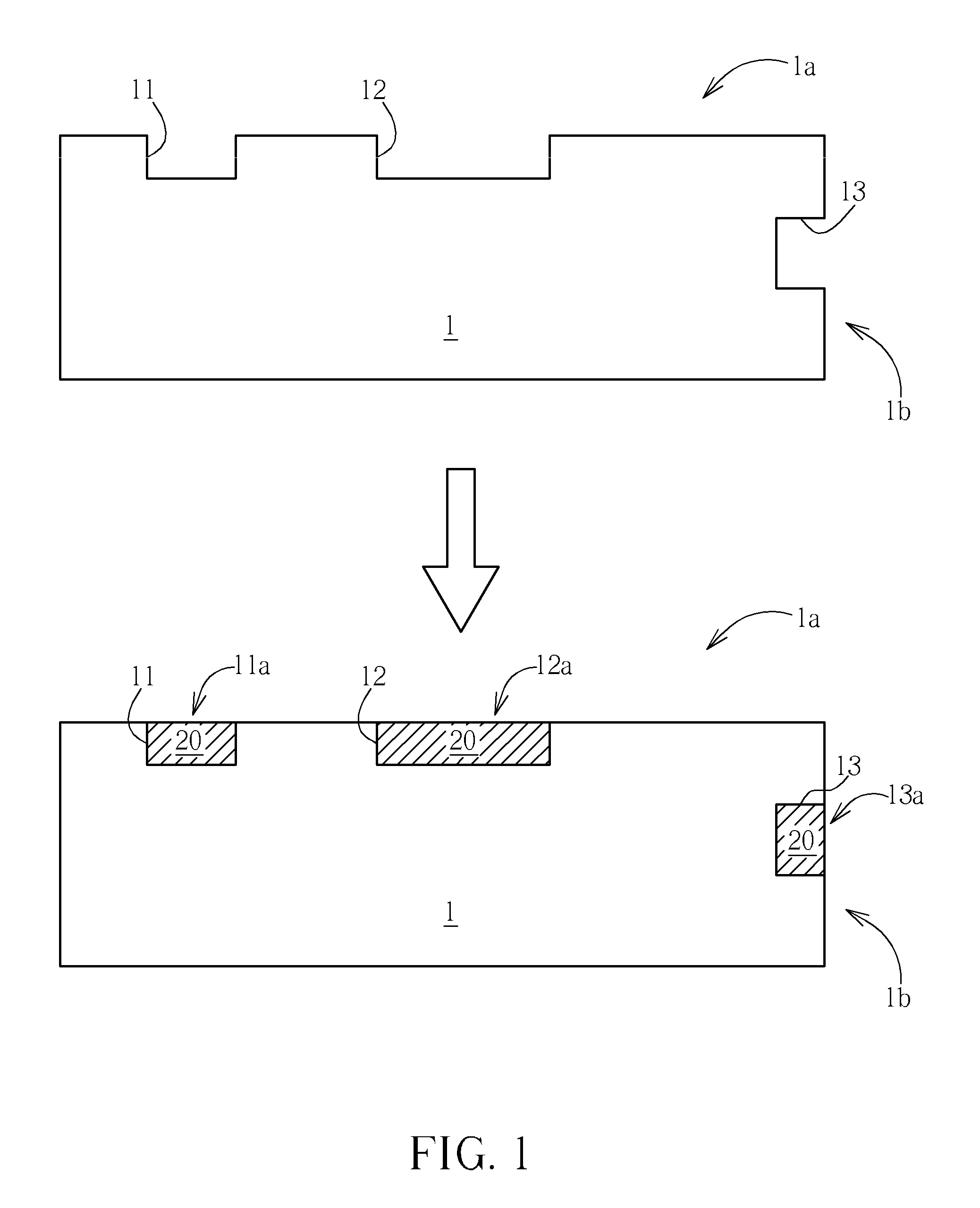
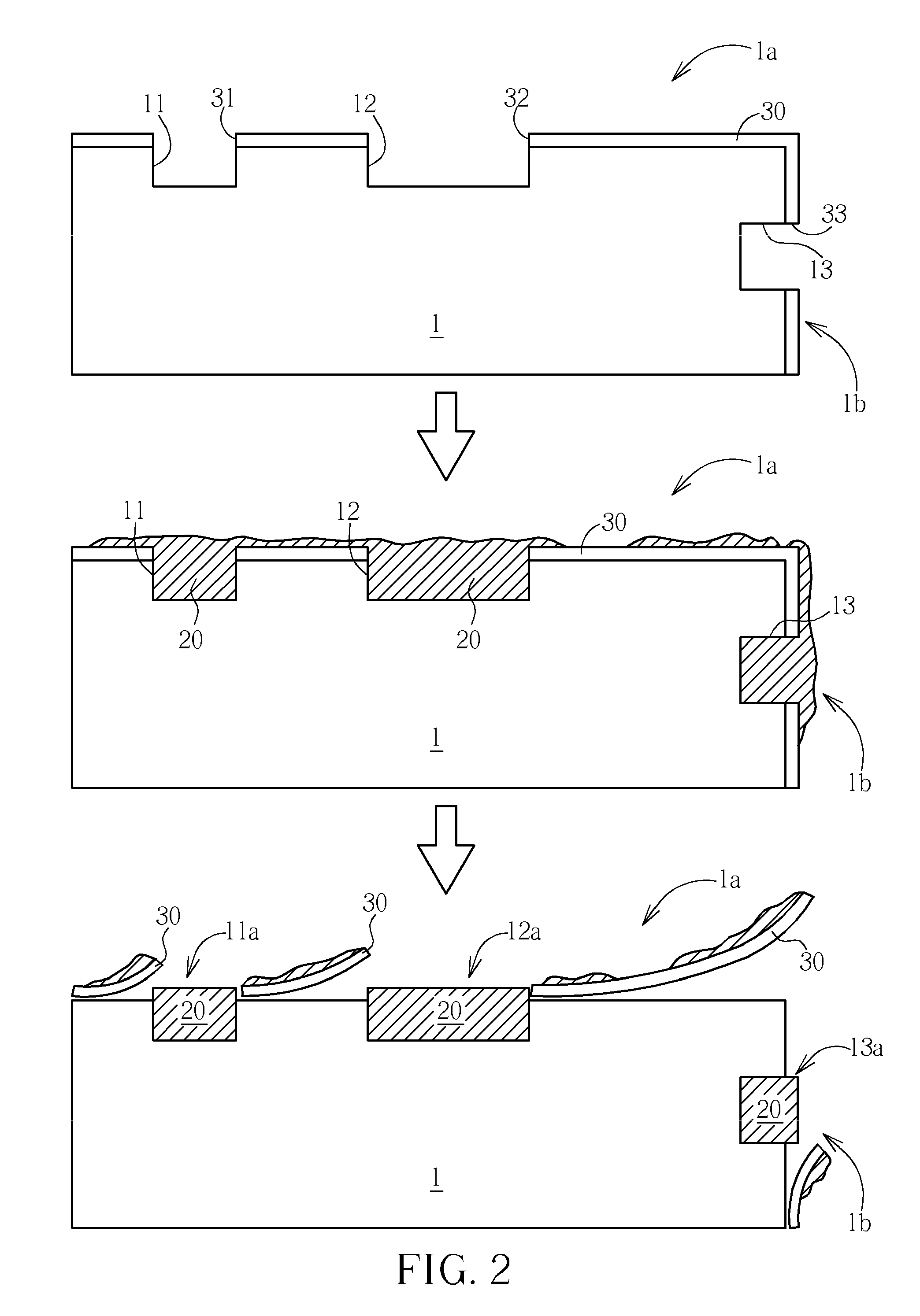
[0019]FIG. 1 is a schematic diagram showing the process of making a molded interconnect device in accordance with one preferred embodiment of this invention. As shown in FIG. 1, an injection molded plastic body 1 is provided having thereon a plurality of patterned circuit trenches 11, 12 and 13. The injection molded plastic body 1 may be formed from polycarbonate, acrylonitrile-butadiene-styrene (ABS), polyet...


PUM

PropertyMeasurementUnit
temperatureaaaaaaaaaa
conductiveaaaaaaaaaa
trench depthsaaaaaaaaaa

Abstract

The present invention provides a method of making a molded interconnect device. The method includes the steps of: injection molding a plastic body having thereon at least one patterned circuit trench structure; and filling a conductive material into the patterned circuit trench structure thereby forming a circuit trace on the plastic body.

Description

BACKGROUND OF THE INVENTION[0001]1. Field of the Invention[0002]The present invention relates generally to a method of fabricating circuit traces on a plastic substrate. More particularly, the present invention relates to a method of making a molded interconnect device.[0003]2. Description of the Prior Art[0004]As known in the art, molded interconnect devices (MIDs) have been used in many applications such as automotive and telecommunication industries. MIDs essentially integrate mechanical and electrical functions into one piece and make an important contribution to design in terms of manufacturability and assembly. Unlike printed circuit boards, which are typically limited to two-dimensional planes, MIDs can implement three-dimensional circuitry. Among other things, a circuit pattern with multiple planes allows better spacing of circuitry, as well as the connected switches and buttons.[0005]Many approaches have been developed for making an MID up to the present. The methods for fa...

Claims


Application Information

Patent Timeline
Patent Type & Authority Patents(United States)
IPC IPC(8): H05K3/02
CPCH05K3/1258H05K1/0284H05K1/0306H05K3/048H05K3/107H05K3/4069Y10T29/4913H05K2203/0191H05K2203/0264Y10T29/49155Y10T29/49126Y10T29/49128Y10T29/49117H05K2201/09118
Inventor YU, CHENG-HUNGLI, CHI-EN
Owner UNIMICRON TECH CORP
Why Eureka
Try Eureka