Low-power USB superspeed device with 8-bit payload and 9-bit frame NRZI encoding for replacing 8/10-bit encoding

a super-speed, low-power technology, applied in the field of low-power universal serialbus (usb) systems, can solve the problems of -memory devices that are already limited in transfer speed, power consumption may be more important than speed, and very power sensitive peripherals

US8166221B2Inactive Publication Date: 2012-04-24SUPER TALENT TECH CORP
3 Cites 21 Cited by

Patent Information

Authority / Receiving Office
US · United States
Patent Type
Patents(United States)
Current Assignee / Owner
Publication Date
2012-04-24
Estimated Expiration
Not applicable · inactive patent

Smart Images

  • Figure 1
    Figure 1
  • Figure 2
    Figure 2
  • Figure 3
    Figure 3
Patent Text Reader

Abstract

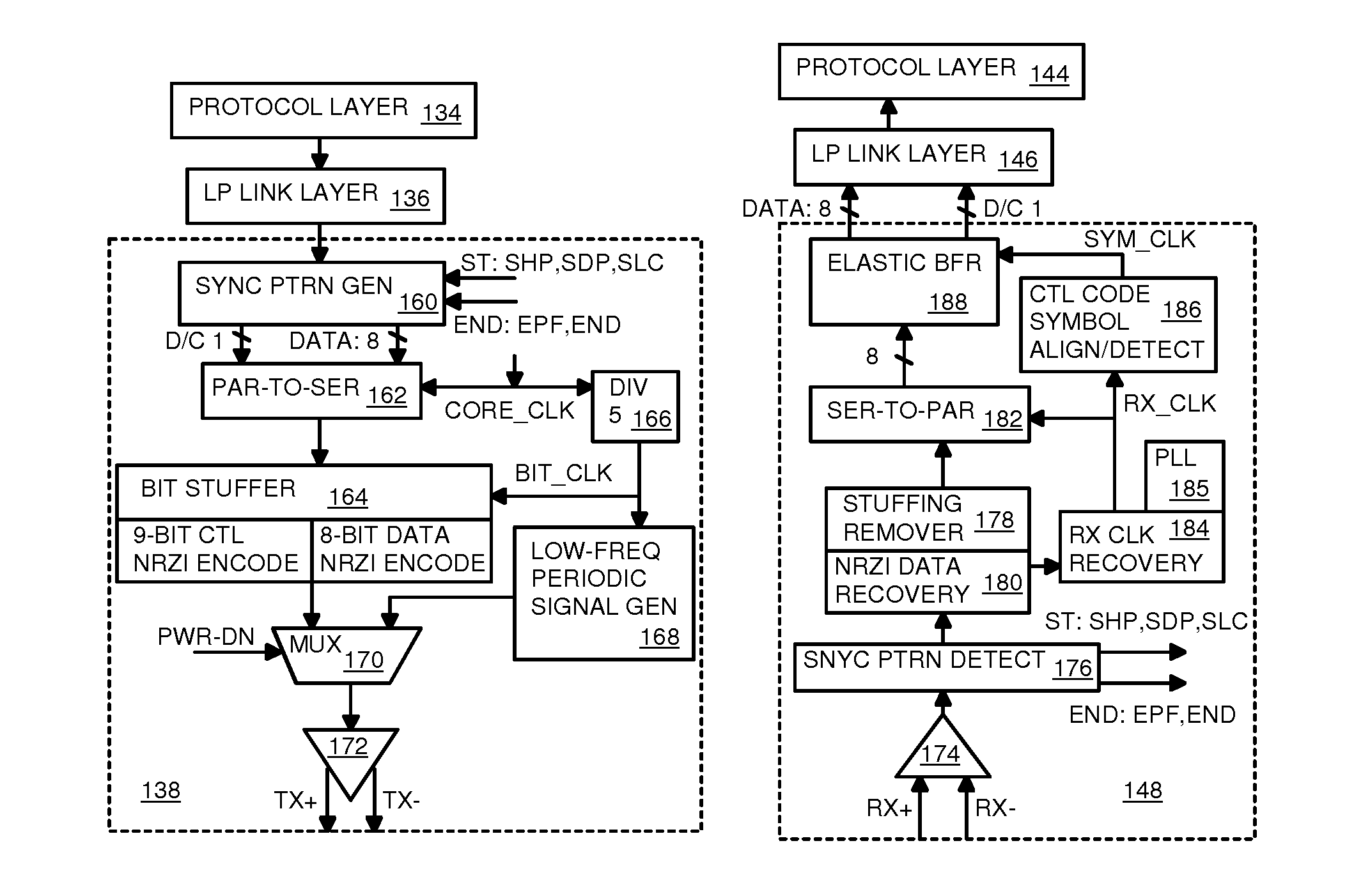
A Low-power flash-memory device uses a modified Universal-Serial-Bus (USB) 3.0 Protocol to reduce power consumption. The bit clock is slowed to reduce power and the need for pre-emphasis when USB cable lengths are short in applications. Data efficiency is improved by eliminating the 8 / 10-bit encoder and instead encoding sync and framing bytes as 9-bit symbols. Data bytes are expanded by bit stuffing only when a series of six ones occurs in the data. Header and payload data is transmitted as nearly 8-bits per data byte while framing is 9-bits per symbol, much less than the standard 10 bits per byte. Low-power link layers, physical layers, and scaled-down protocol layers are used. A card reader converter hub allows USB hosts to access low-power USB devices. Only one flash device is accessed, reducing power compared with standard USB broadcasting to multiple devices.
Need to check novelty before this filing date? Find Prior Art

Description

RELATED APPLICATION

[0001] This application is a continuation-in-part of the co-pending application for “PCI EXPRESS-COMPATIBLE CONTROLLER AND INTERFACE FOR FLASH MEMORY”, U.S. Ser. No. 12 / 254,428, filed on Oct. 20, 2008, which is a Division of “PCI EXPRESS-COMPATIBLE CONTROLLER AND INTERFACE FOR FLASH MEMORY”, U.S. application Ser. No. 10 / 803,597, filed on Mar. 17, 2004, now U.S. Pat. No. 7,457,897.

[0002] This application is also a CIP of the co-pending U.S. patent application for “Low-Power Extended USB Flash Device without Polling”, U.S. application Ser. No. 11 / 925,933, filed on Oct. 27, 2007.

[0003] This application is a continuation-in-part (CIP) of co-pending U.S. patent application for “HIGH-LEVEL BRIDGE FROM PCIE TO EXTENDED USB” Ser. No. 11 / 926,636, filed on Oct. 29, 2007.

[0004] This application is also a CIP of co-pending U.S. patent application for “Chained DMA for Low-Power Extended USB Flash Device Without Polling”, U.S. application Ser. No. 11 / 928,124, filed on Oct. 30, 2007...

Examples

Embodiment Construction

[0046]The present invention relates to an improvement in low-power USB systems. The following description is presented to enable one of ordinary skill in the art to make and use the invention as provided in the context of a particular application and its requirements. Various modifications to the preferred embodiment will be apparent to those with skill in the art, and the general principles defined herein may be applied to other embodiments. Therefore, the present invention is not intended to be limited to the particular embodiments shown and described, but is to be accorded the widest scope consistent with the principles and novel features herein disclosed.

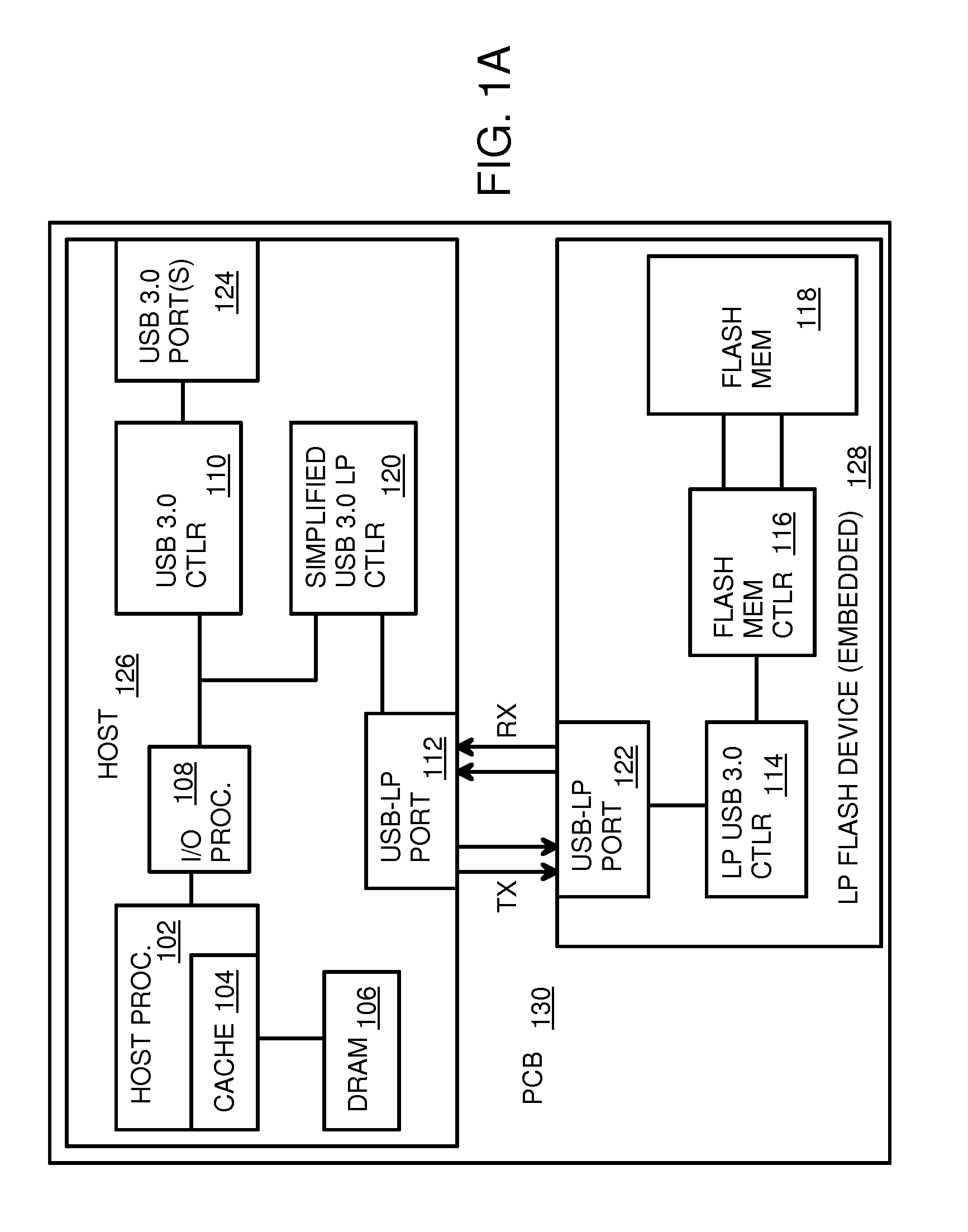
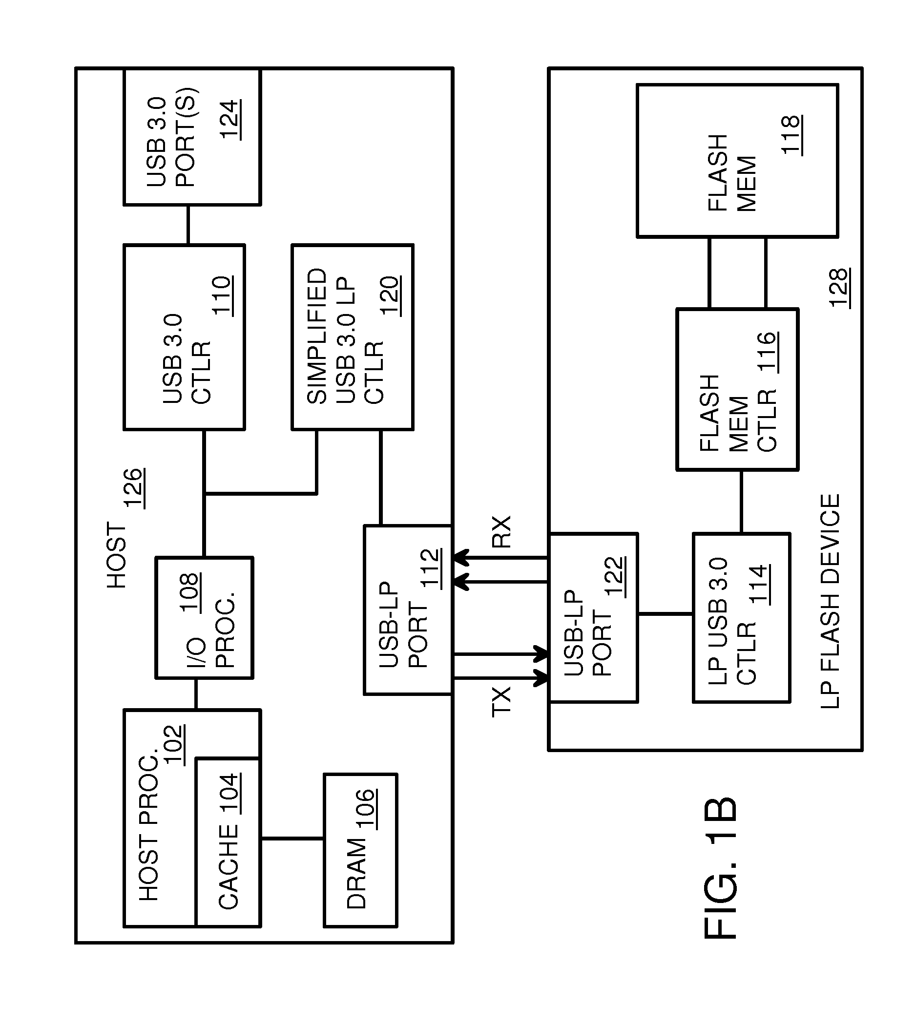
[0047]FIG. 1A is a block diagram of an embedded low-power flash device. Host 126 and low-power flash device 128 are both integrated onto the same PCB 130, such as a motherboard or other circuit board. Host 126 has host processor 102 with cache memory 104 that read data and instructions from dynamic-random-access memory (DRAM) 10...