Supercharge Your Innovation With Domain-Expert AI Agents!

Semiconductor package

a technology of semiconductor chips and packages, applied in the direction of semiconductor/solid-state device details, semiconductor devices, electrical apparatus, etc., can solve the problems of inability to stack semiconductor chips and perform wire bonding processes, and inability to increase the capacity of a semiconductor chip itself, so as to prevent inferior mounting of a semiconductor chip

Inactive Publication Date: 2013-08-27
SK HYNIX INC
View PDF4 Cites 0 Cited by
  • Summary
  • Abstract
  • Description
  • Claims
  • Application Information

AI Technical Summary

Benefits of technology

This approach ensures secure mounting and reliable electrical connections of warped semiconductor chips, facilitating high-density stacking and improved mounting reliability by preventing further warpage and ensuring uniform contact with the substrate.

Problems solved by technology

However, there limitations to increasing the capacity of a semiconductor chip itself.
When a semiconductor chip is warped with the edge portions bent upward, the warpage prevents the entire surface of the semiconductor chip from being attached to a substrate, and, when the chip surface is not securely attached to the substrate, it will cause difficulties in the subsequent wire bonding process.
It may be impossible not only to stack semiconductor chips but also to perform a wire bonding process due to the warped semiconductor chips.

Method used


Image

  • Semiconductor package
  • Semiconductor package
  • Semiconductor package

Examples


Embodiment Construction

[0036]Hereafter, specific embodiments of the present invention will be described in detail with reference to the accompanying drawings.

[0037]It is to be understood herein that the drawings are not necessarily to scale and in some instances proportions may have been exaggerated in order to more clearly depict certain features of the invention.

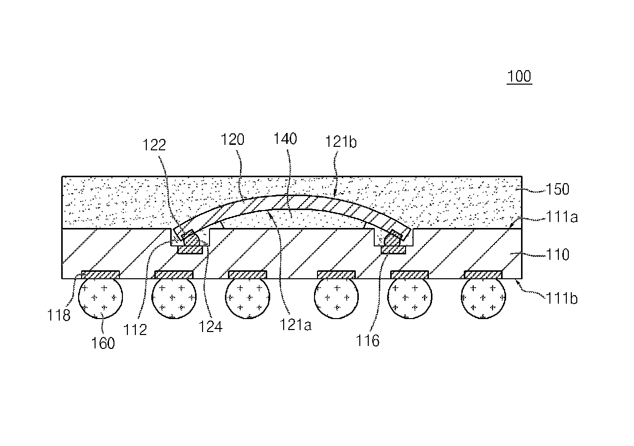
[0038]FIG. 1 is a cross-sectional view illustrating a semiconductor package in accordance with an embodiment of the present invention, and FIG. 2 is a plan view illustrating the substrate shown in FIG. 1.

[0039]Referring to FIGS. 1 and 2, a semiconductor package 100 in accordance with an embodiment of the present invention includes a substrate 110, and a semiconductor chip 120 which is mounted to the substrate 110. Also, the semiconductor package 100 in accordance with an embodiment of the present invention further includes an adhesive component 140, an encapsulation component 150, and external mounting members 160.

[0040]The substrate 110 may be ...


PUM


Abstract

A semiconductor package includes a substrate having an upper surface and a lower surface which faces away from the upper surface, and possessing a recess which is defined on the upper surface; and a semiconductor chip mounted to the upper surface of the substrate, having one surface which faces the upper surface and the other surface which faces away from the one surface, and warped in a smile shape such that a warped edge portion of the semiconductor chip is inserted into the recess.

Description

CROSS-REFERENCE TO RELATED APPLICATIONS[0001]The present application claims priority to Korean patent application number 10-2010-0100740 filed on Oct. 15, 2010 and Korean patent application number 10-2011-0096144 filed on Sep. 23, 2011, which are incorporated herein by reference in their entireties.BACKGROUND OF THE INVENTION[0002]The present invention relates generally to a semiconductor package, and more particularly to a semiconductor package which is realized using the warpage of a semiconductor chip.[0003]In general, a semiconductor chip in a semiconductor package is adhered to the upper surface of a substrate, which is electrically connected to the semiconductor chip by wires, and the upper surface of the substrate is sealed to cover the semiconductor chip and the wires.[0004]In keeping with the modern semiconductor products requiring increasingly large capacity, a semiconductor chip with a larger capacity needs to be mounted in a semiconductor package. However, there limitati...

Claims


Application Information

Patent Timeline
Patent Type & Authority Patents(United States)
IPC IPC(8): H01L23/02H01L21/00H01L21/44H01L29/40H01L23/52H01L23/48H01L23/34
CPCH01L24/73H01L25/0657H01L29/0657H01L23/13H01L23/3128H01L24/05H01L24/06H01L24/13H01L24/16H01L24/29H01L24/32H01L2224/0401H01L2224/05548H01L2224/06155H01L2224/131H01L2224/13144H01L2224/16227H01L2224/16237H01L2224/2919H01L2224/32145H01L2224/32225H01L2224/73203H01L2224/73204H01L2225/06517H01L2225/06555H01L2924/01079H01L2924/1515H01L2924/15311H01L2924/3511H01L2924/014H01L2924/01033H01L2224/02379H01L23/49816H01L2924/00013H01L2224/13099H01L2224/13599H01L2224/05599H01L2224/05099H01L2224/29099H01L2224/29599H01L2224/16225H01L2924/00H01L2924/10155H01L2924/181
Inventor ROH, HEE RA
Owner SK HYNIX INC
Features
  • R&D
  • Intellectual Property
  • Life Sciences
  • Materials
  • Tech Scout
  • Unparalleled Data Quality
  • Higher Quality Content
  • 60% Fewer Hallucinations
Learn More