Micro and millimeter waves circuit

a micro- and millimeter-wave technology, applied in the field of communication technologies, can solve problems such as the inability to implement large-scale circuit design

Active Publication Date: 2015-03-24
HUAWEI TECH CO LTD
View PDF12 Cites 1 Cited by
  • Summary
  • Abstract
  • Description
  • Claims
  • Application Information

AI Technical Summary

Benefits of technology

[0010]It may be seen from the foregoing technical solutions provided by the embodiments of the present invention that, the circuit module is supported in the form of disposing the projecting part on the base of the heat substrate, so that two or even more conductor layers may be disposed in the multi-layer circuit board, and the more conductor layers can bear more wiring. In this way, the large-scale circuit design may be implemented on the circuit board with multiple layers.

Problems solved by technology

The circuit board adopted in the existing MMW circuit is only disposed with one layer of conductors, so large-scale circuit design cannot be implemented.

Method used


Image

  • Micro and millimeter waves circuit
  • Micro and millimeter waves circuit
  • Micro and millimeter waves circuit

Examples


Embodiment Construction

[0021]To facilitate understanding of the embodiments of the present invention, explanation and illustration are further given in the following by taking several specific embodiments as examples with reference to the accompanying drawings, and each embodiment is not intended to limit the embodiments of the present invention.

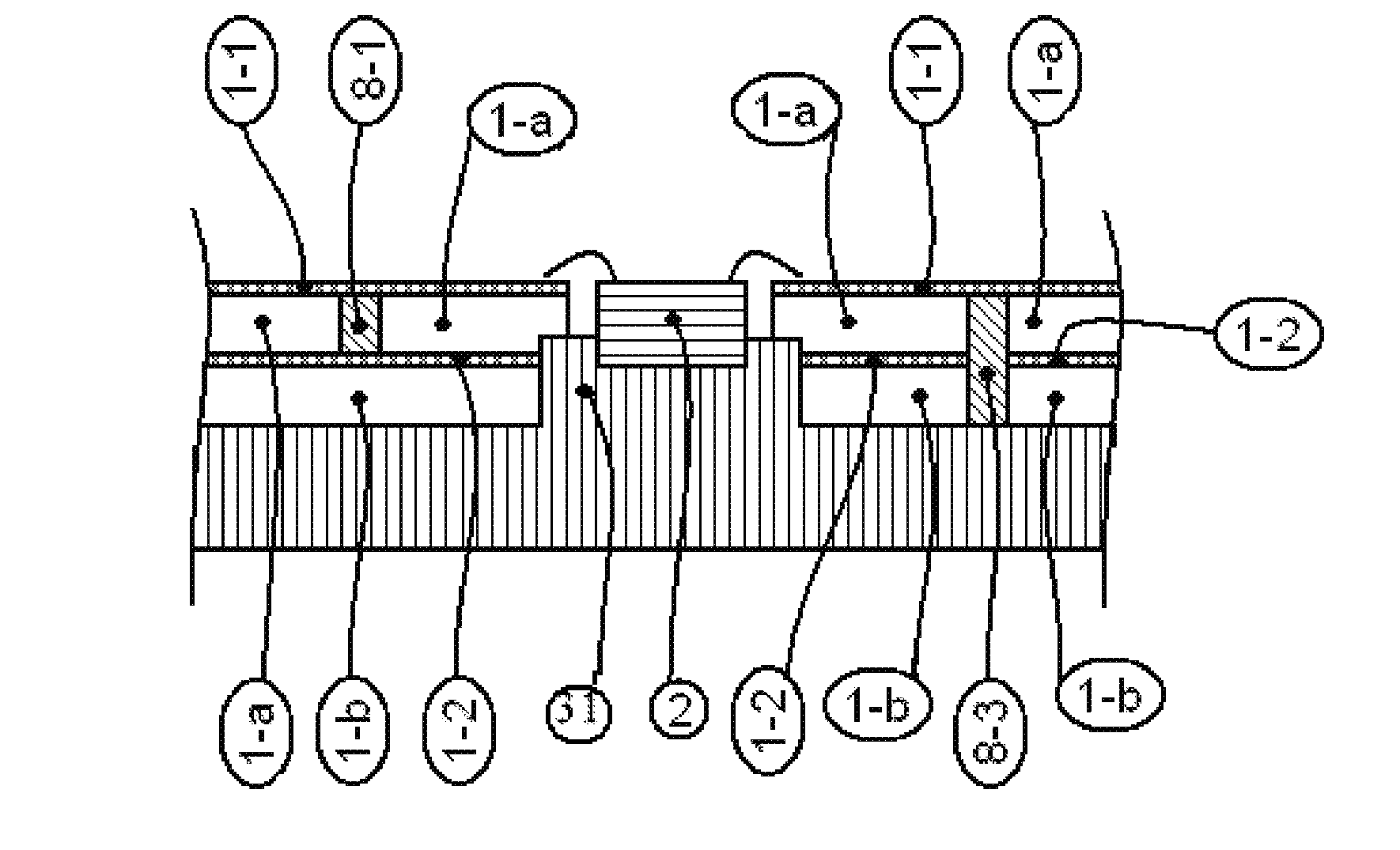
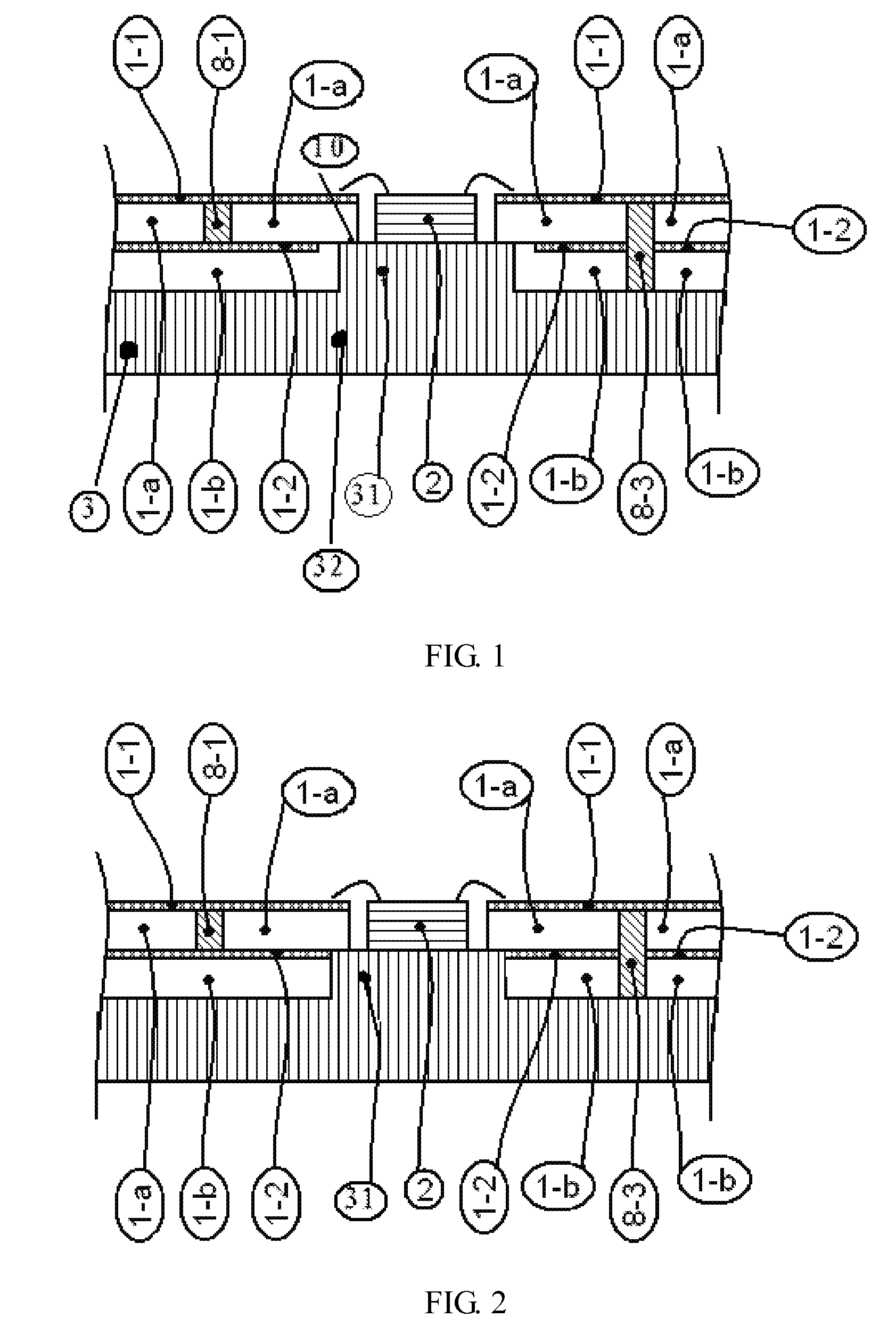
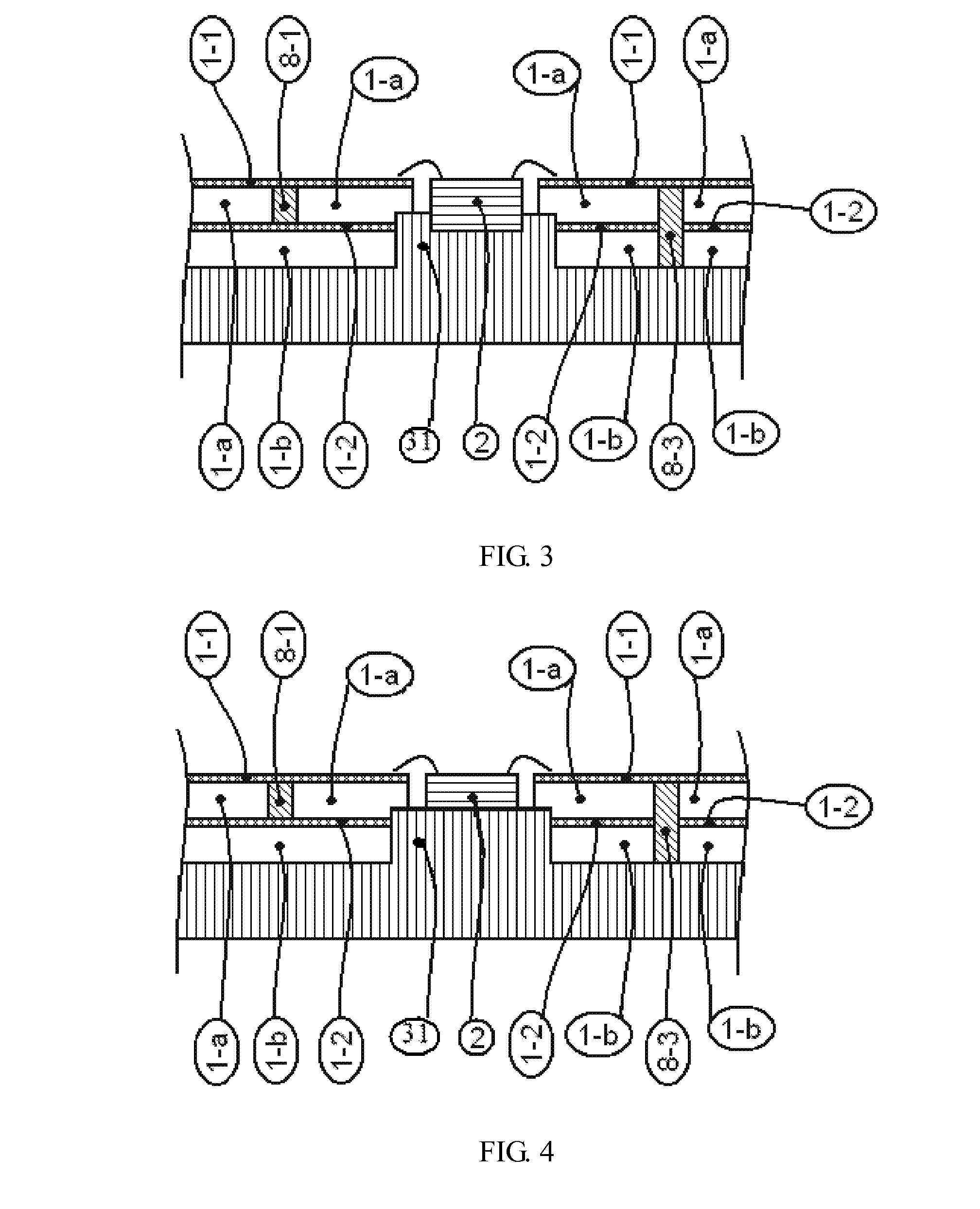
[0022]As shown in FIG. 1, the present invention provides an embodiment of a micro and millimeter waves circuit, including: a multi-layer circuit board, a heat substrate 3, and a circuit module 2. The multi-layer circuit board is opened with a window. The heat substrate 3 includes a base 32. The multi-layer circuit board is attached to the base 32. The heat substrate 3 further includes a projecting part 31 extending from the base into the window of the multi-layer circuit board. The circuit module 2 is received in the window and placed on the projecting part 3. The circuit module 2 is electrically connected with an outer conductor layer 1-1 of the multi-layer circu...


PUM


Abstract

Embodiments of the present invention provide a micro and millimeter waves circuit, including: a multi-layer circuit board, a heat substrate, and a circuit module. The multi-layer circuit board is opened with a window. The heat substrate includes a base. The multi-layer circuit board is attached to the base. The heat substrate further includes a projecting part extending from the base into the window of the multi-layer circuit board. The circuit module is received in the window and placed on the projecting part. The circuit module is electrically connected with an outer conductor layer of the multi-layer circuit board.

Description

CROSS-REFERENCE TO RELATED APPLICATIONS[0001]This application is a continuation of International Application No. PCT / CN2011 / 073724, filed on May 6, 2011, which claims priority to Chinese Patent Application No. 201010241422.X, filed on Jul. 31, 2010, both of which are hereby incorporated by reference in their entireties.FIELD OF THE INVENTION[0002]The present invention relates to the field of communications technologies, and in particular, to a micro and millimeter waves circuit.BACKGROUND OF THE INVENTION[0003]As shown in FIG. 9, an existing MMW (Micro and Millimeter Waves, micro and millimeter waves) circuit includes a circuit board (for example, a PCB). The circuit board is placed on a heat substrate (a metal block with heat conductivity, such as a copper block or an aluminum block). The circuit board is opened with a window. A bare chip is placed in the window, and placed on the heat substrate.[0004]The bare chip is adhered on the heat substrate through electrical conduction mate...

Claims


Application Information

Patent Timeline
Patent Type & Authority Patents(United States)
IPC IPC(8): H05K1/18H01L23/13H01L23/367H01L23/66H05K1/02
CPCH01L23/3677H05K1/021H01L23/66H01L23/13H05K1/0243H05K2201/09054H01L2223/6627H01L2224/48227
Inventor LUO, BINGMARCONI, FRANCO
Owner HUAWEI TECH CO LTD
Why Eureka
Try Eureka