Method for assembling at least one chip using a fabric, and fabric including a chip device

a technology of fabric and chip, applied in the field of fabric including electronic chips, can solve the problems of complex implementation of secure methods, unsuitable for flexible structure integration, drawback of using rigid mechanical supports, etc., and achieve the effect of simple manner

Active Publication Date: 2015-07-28
COMMISSARIAT A LENERGIE ATOMIQUE ET AUX ENERGIES ALTERNATIVES
View PDF23 Cites 60 Cited by
  • Summary
  • Abstract
  • Description
  • Claims
  • Application Information

AI Technical Summary

Benefits of technology

[0006]It is thus sought to incorporate electronic chip devices in a fabric in simple manner without precautions being required when performing weaving. For this, it is sought in particular to produce a chip device that can be incorporated in easy manner between two parallel taut threads, in particular belonging to a finished fabric.

Problems solved by technology

It does however present the main drawback of using a rigid mechanical support, which is particularly unsuitable for integration in flexible structures.
These securing methods are complex to implement on account of the small size of the chip devices.

Method used


Image

  • Method for assembling at least one chip using a fabric, and fabric including a chip device
  • Method for assembling at least one chip using a fabric, and fabric including a chip device
  • Method for assembling at least one chip using a fabric, and fabric including a chip device

Examples


Embodiment Construction

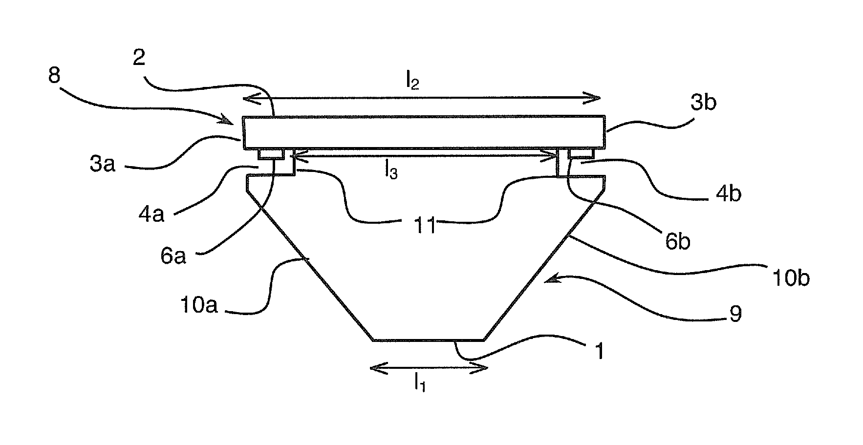
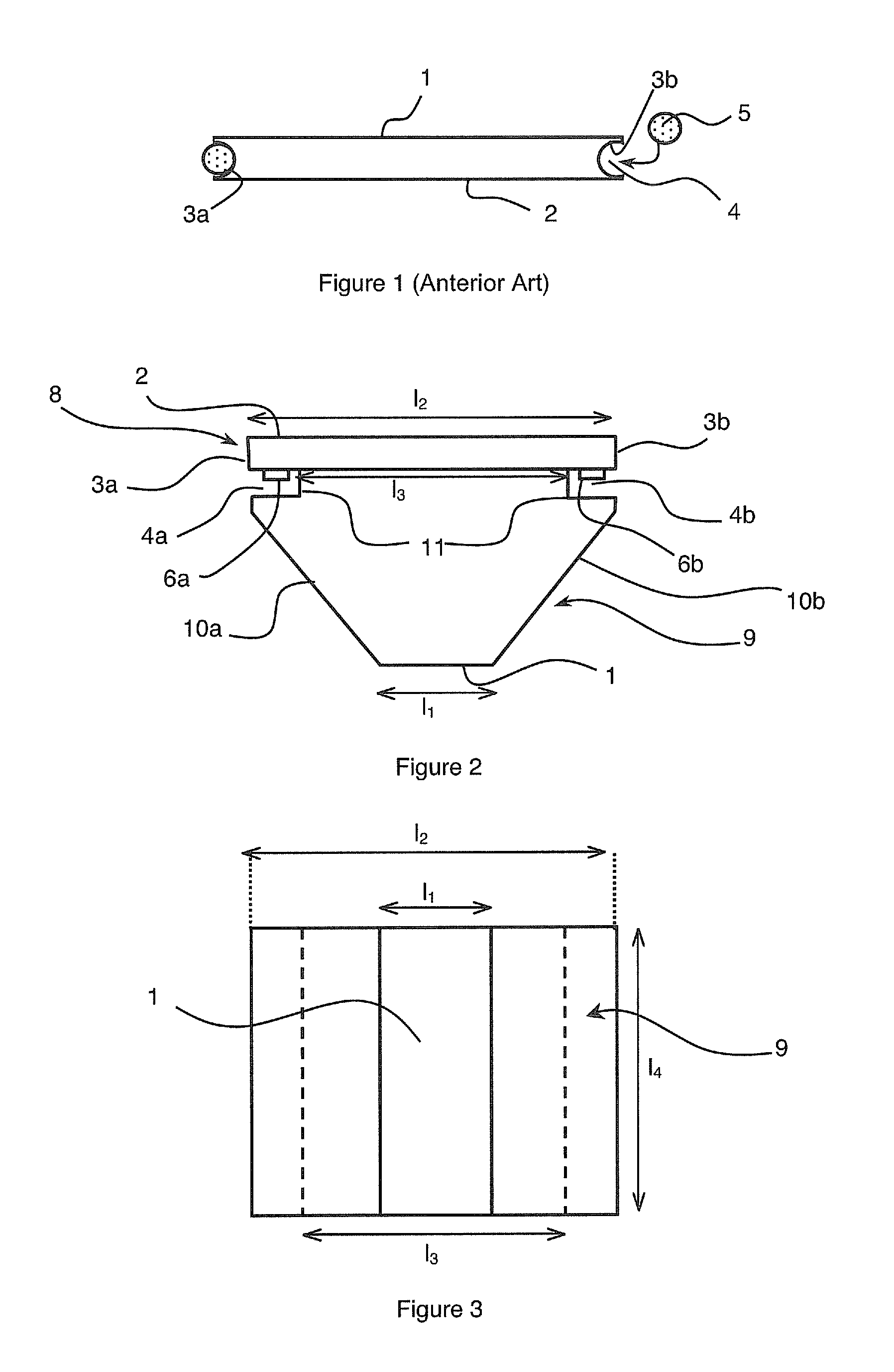
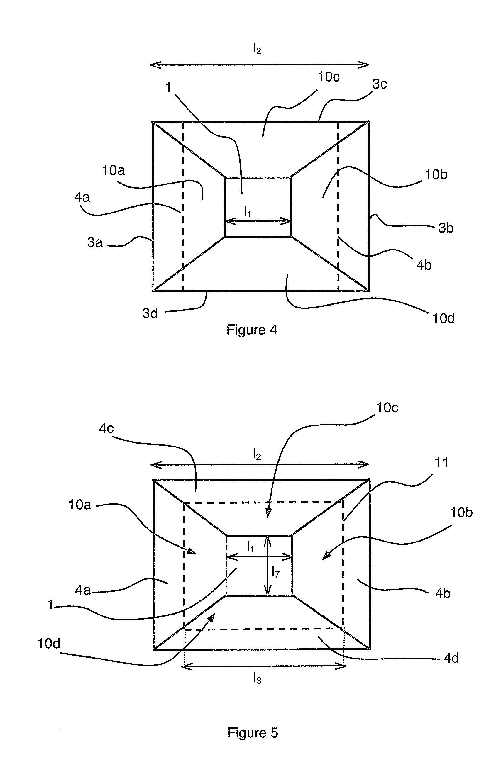
[0019]As indicated in the foregoing, it is sought to produce an electronic chip device provided with grooves for insertion of threads that is easily incorporable in a fabric. These chip devices will in particular be able to be incorporated in a finished fabric. In other words, they will not have to be secured to threads that are subsequently used to weave the fabric.

[0020]As a general rule, a fabric is formed by warp threads that are substantially parallel to one another and by weft threads that are substantially parallel to one another and that cross the warp threads. Two consecutive warp threads and two consecutive weft threads form a stitch more often than not having the general shape of a parallelogram. Other types of fabrics and stitches can naturally be envisaged.

[0021]A chip device as described in greater detail in the following comprises a part presenting a penetrating profile, designed to be inserted in a stitch of the fabric and to separate the threads forming the stitch u...


PUM

PropertyMeasurementUnit
thicknessaaaaaaaaaa
thicknessaaaaaaaaaa
distanceaaaaaaaaaa

Abstract

A method for assembling a device on two substantially parallel taut threads. The device includes an electronic chip and two substantially parallel grooves open on opposite sides of the device. The distance separating the grooves corresponds to the distance separating the threads. The device presents a penetrating shape along an axis perpendicular to the plane of the grooves, having a base at the level of the grooves and an apex of smaller size than the distance separating the threads. The method includes the steps consisting in placing the apex of the device between the two threads; in moving the device between the two threads resulting in the threads being separated from one another by the penetrating shape of the device; and in continuing movement of the device until the threads penetrate into the grooves reverting to their initial separation distance.

Description

BACKGROUND OF THE INVENTION[0001]The invention relates to a device including an electronic chip and comprising two open grooves on opposite sides of the device.STATE OF THE ART[0002]Numerous techniques exist at the present time to connect microelectronic chips mechanically and electrically to one another. A conventional technique consists in making a rigid mechanical connection between the chips, once the chips have been formed on a substrate and released by dicing. The chips, then fixed on a rigid support, are then electrically connected before a protective coating is formed. This approach, consisting in making connection on a rigid support, is conventionally used when a great complexity exists in connection of the chips. It does however present the main drawback of using a rigid mechanical support, which is particularly unsuitable for integration in flexible structures.[0003]The document WO2008 / 025889 filed by the applicant describes a microelectronic chip, as illustrated in FIG. ...

Claims


Application Information

Patent Timeline
Patent Type & Authority Patents(United States)
IPC IPC(8): H05K7/06D03D9/00D03D1/00H01L29/06H05K13/00F21V21/00D03D15/00H01L23/00H01L25/065H01L25/00
CPCH01L29/0657D03D1/0088D03D9/00D03D15/00H01L24/49H01L24/72D10B2401/16D10B2401/18D10B2501/00H01L25/0655H01L25/50H01L2224/4807H01L2224/49H01L2224/858H01L2924/01014H01L2924/01029H01L2924/01058H01L2924/01079H01L2924/12041Y10T29/49002H01L2924/00H01L2924/00014H01L2924/14H01L24/48D03D15/25H01L2224/45099
Inventor VICARD, DOMINIQUEBRUN, JEAN
Owner COMMISSARIAT A LENERGIE ATOMIQUE ET AUX ENERGIES ALTERNATIVES
Why Eureka
Try Eureka