Micro pick up array with integrated pivot mount

a technology of micro-opt-in arrays and pivot mounts, which is applied in the direction of gripping heads, manufacturing tools, and semiconductor/solid-state device details, etc., can solve the problems of difficulty and cost associated with manufacturing miniaturized devices, mems or quartz-based oscillators, and commercialization of miniaturized devices

Active Publication Date: 2016-04-19
APPLE INC
View PDF77 Cites 35 Cited by
  • Summary
  • Abstract
  • Description
  • Claims
  • Application Information

AI Technical Summary

Problems solved by technology

The feasibility of commercializing miniaturized devices such as radio frequency (RF) microelectromechanical systems (MEMS) microswitches, light-emitting diode (LED) display systems, and MEMS or quartz-based oscillators is largely constrained by the difficulties and costs associated with manufacturing those devices.

Method used


Image

  • Micro pick up array with integrated pivot mount
  • Micro pick up array with integrated pivot mount
  • Micro pick up array with integrated pivot mount

Examples


Embodiment Construction

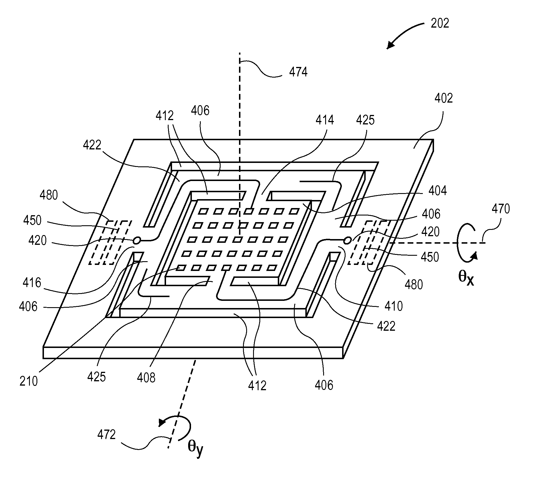
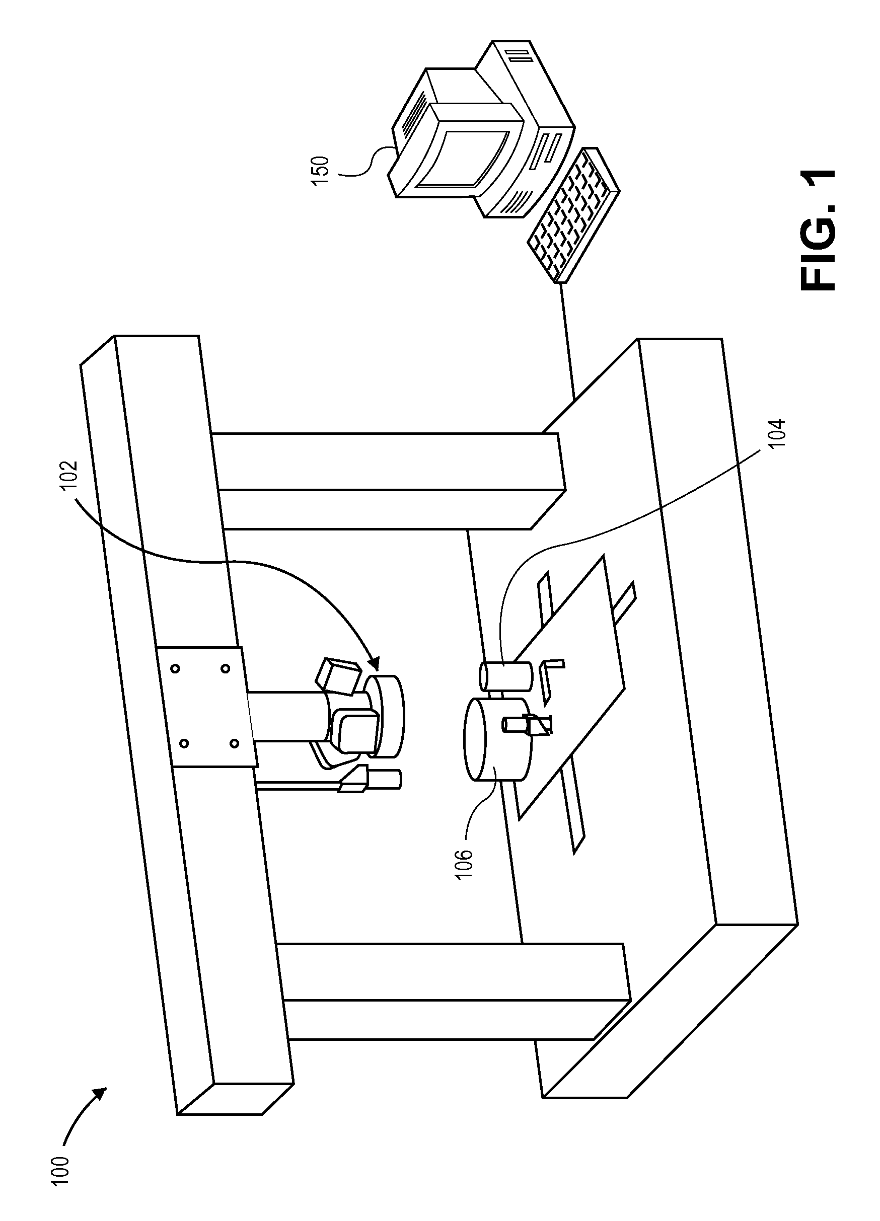
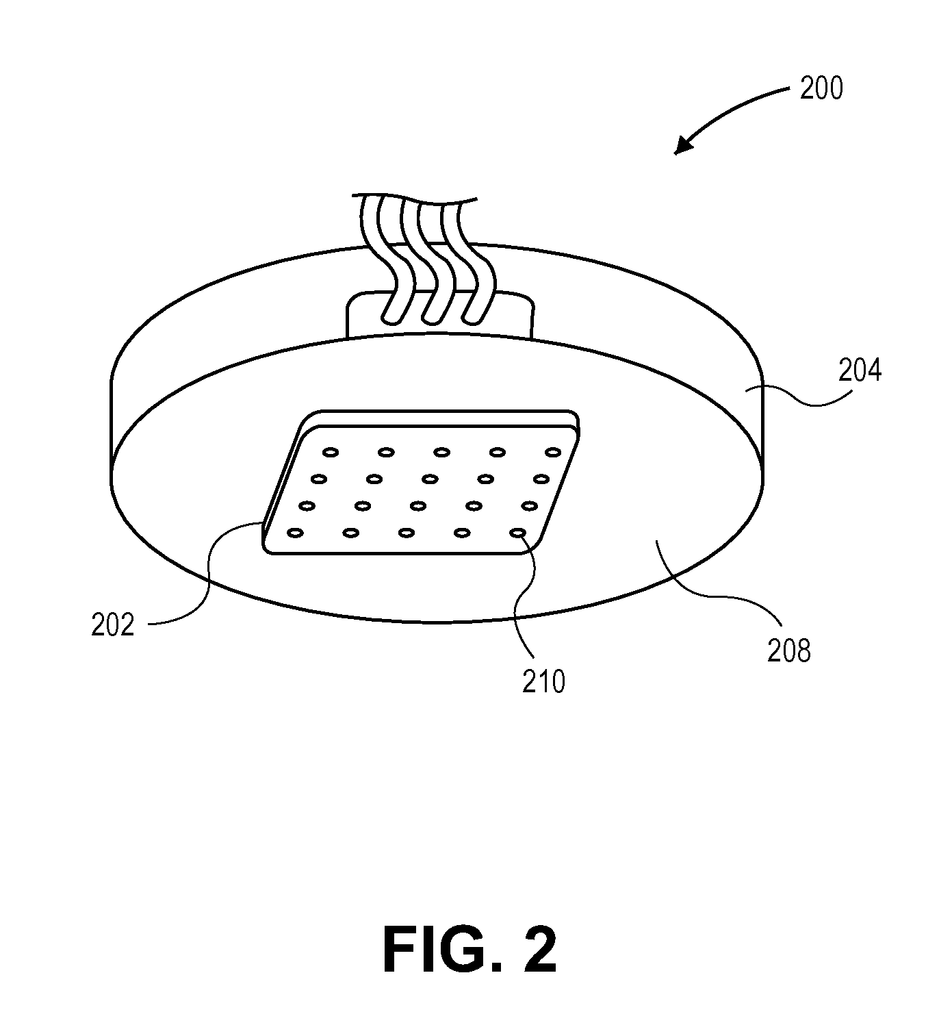
[0052]Embodiments of the present invention describe systems and methods for transferring a micro device or an array of micro devices from a carrier substrate. For example, the micro devices or array of micro devices may be any of the micro LED device structures illustrated and described in related U.S. patent application Ser. Nos. 13 / 372,222, 13 / 436,260, 13 / 458,932, and 13 / 625,825. While some embodiments of the present invention are described with specific regard to micro LED devices, the embodiments of the invention are not so limited and certain embodiments may also be applicable to other micro LED devices and micro devices such as diodes, transistors, ICs, and MEMS.

[0053]In various embodiments, description is made with reference to the figures. However, certain embodiments may be practiced without one or more of these specific details, or in combination with other known methods and configurations. In the following description, numerous specific details are set forth, such as spec...


PUM

PropertyMeasurementUnit
surface areaaaaaaaaaaa
widthaaaaaaaaaa
distanceaaaaaaaaaa

Abstract

Systems and methods for transferring a micro device from a carrier substrate include, in an embodiment, a micro pick up array structure to allow the micro pick up array to automatically align with the carrier substrate. Deflection of the micro pick up array may be detected to control further movement of the micro pick up array.

Description

BACKGROUND[0001]1. Field[0002]The present invention relates to micro devices. More particularly, embodiments of the present invention relate to systems and methods for transferring a micro device from a carrier substrate.[0003]2. Background Information[0004]The feasibility of commercializing miniaturized devices such as radio frequency (RF) microelectromechanical systems (MEMS) microswitches, light-emitting diode (LED) display systems, and MEMS or quartz-based oscillators is largely constrained by the difficulties and costs associated with manufacturing those devices. Manufacturing processes typically include wafer based processing and transferring techniques.[0005]Device transferring processes include transfer from a transfer wafer to a receiving wafer. One such implementation is “direct printing” involving one bonding step of an array of devices from a transfer wafer to a receiving wafer, followed by removal of the transfer wafer. Another such implementation is “transfer printing”...

Claims


Application Information

Patent Timeline
Patent Type & Authority Patents(United States)
IPC IPC(8): B23P19/00B25J7/00B81C99/00B25J15/00H01L23/00
CPCB25J15/0085B25J7/00B81C99/002H01L24/75H01L2224/7598Y10T29/53174
Inventor GOLDA, DARIUSZHIGGINSON, JOHN A.BIBL, ANDREAS
Owner APPLE INC
Why Eureka
Try Eureka